|
|
|
PDF BU4066BC Data sheet ( Hoja de datos )
| Número de pieza | BU4066BC | |
| Descripción | Quad analog switch | |
| Fabricantes | ROHM Semiconductor | |
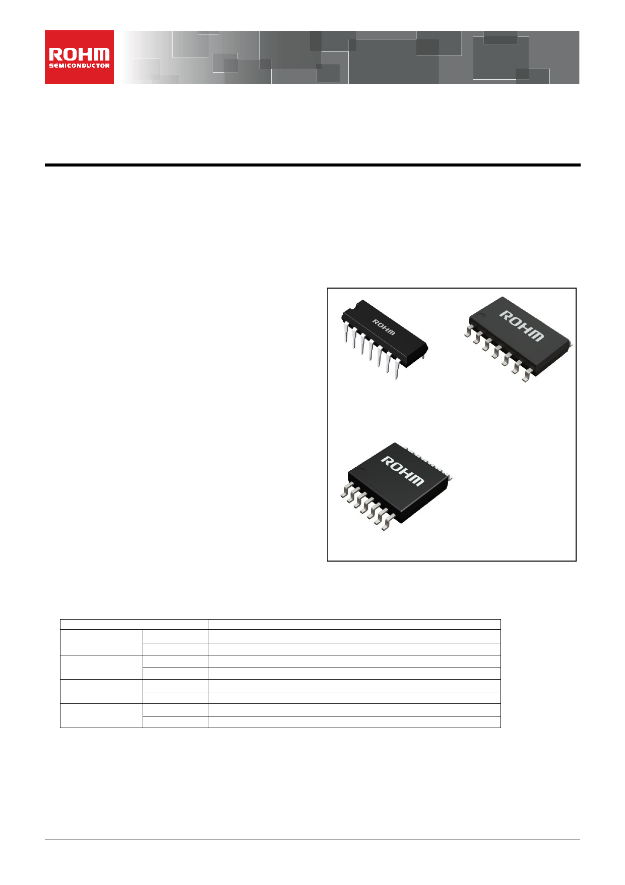
| Logotipo | ||
Hay una vista previa y un enlace de descarga de BU4066BC (archivo pdf) en la parte inferior de esta página. Total 19 Páginas | ||
|
No Preview Available !
Datasheet
General Purpose CMOS Logic IC
Quad-Analog Switch
BU4066BC BU4066BCF BU4066BCFV
General Description
The BU4066BC series ICs each contain 4 independent
switches capable of controlling either digital or analog
signals.
Features
Low Power Consumption
Wide Operating Supply Voltage Range
Key Specifications
Operating Supply Voltage Range:
3V to 18V
Input Voltage Range:
VEE to VDD
Operating Temperature Range: -40°C to +85°C
Packages
DIP14
SOP14
SSOP-B14
W(Typ) x D(Typ) x H(Max)
19.40mm x 6.50mm x 7.95mm
8.70mm x 6.20mm x 1.71mm
5.00mm x 6.40mm x 1.35mm
DIP14
SOP14
Truth Table
Inputs
CONT.A
CONT.B
CONT.C
CONT.D
H
L
H
L
H
L
H
L
SSOP-B14
Switches
SWA is turned on. (1pin-2pin)
SWA is turned off. (1pin-2pin)
SWB is turned on. (3pin-4pin)
SWB is turned off. (3pin-4pin)
SWC is turned on. (8pin-9pin)
SWC is turned off. (8pin-9pin)
SWD is turned on. (10pin-11pin)
SWD is turned off. (10pin-11pin)
〇Product structure : Silicon monolithic integrated circuit
.www.rohm.com
© 2014 ROHM Co., Ltd. All rights reserved.
TSZ22111 • 14 • 001
〇This product has no designed protection against radioactive rays
1/16
TSZ02201-0RDR0GZ00270-1-2
12.Nov.2014 Rev.001
1 page 
BU4066BC BU4066BCF BU4066BCFV
Waveforms of Switching Characteristics
IN/OUT
(INPUT)
VDD
VEE
50%
50%
OUT/IN
(OUTPUT)
50%
50%
tPLH
tPHL
Figure 1. Propagation Delay Time IN→OUT(tPHZ,tPLZ)
Input/Output Waveform
CONT
(INPUT)
VDD
VEE
50%
50%
OUT/IN
(OUTPUT)
50%
90%
tPZH
tPHZ
Figure 3. Propagation Delay Time CONT→OUT (tPZH,tPHZ)
Input/Output Waveform
VDD
P.G
IN/OUT
CONT
OUT/IN
RL
CL
VEE
VEE
Figure 2. Propagation Delay Time IN→OUT(tPHZ,tPLZ)
Test Circuit
P.G
VDD
IN/OUT
CONT
OUT/IN
RL CL
Figure 4.
VEE
VEE
Propagation Delay Time CONT→OUT (tPZH,tPHZ)
Test Circuit
CONT
(INPUT)
VDD
VEE
OUT/IN
(OUTPUT)
50%
50%
50%
10%
P.G
VDD
VDD
CONT
RL CL
IN/OUT
OUT/IN
VEE
tPZL
tPLZ
Figure 5. Propagation Delay Time CONT→OUT (tPZL,tPLZ)
Input/Output Waveform
VDD
Figure 6. Propagation Delay Time CONT→OUT (tPZL,tPLZ)
Test Circuit
www.rohm.com
© 2014 ROHM Co., Ltd. All rights reserved.
TSZ22111 • 15 • 001
VIN= VDD/2
IN/OUT
CONT
OUT/IN
RL
VOUT
RON = RL(VIN/VOUT -1)
VEE
VEE
Figure 7. ON Resistance (RON) Test Circuit
5/16
TSZ02201-0RDR0GZ00270-1-2
12.Nov.2014 Rev.001
5 Page 
BU4066BC BU4066BCF BU4066BCFV
Operational Notes – continued
11. Unused Input Pins
Input pins of an IC are often connected to the gate of a MOS transistor. The gate has extremely high impedance and
extremely low capacitance. If left unconnected, the electric field from the outside can easily charge it. The small
charge acquired in this way is enough to produce a significant effect on the conduction through the transistor and
cause unexpected operation of the IC. So unless otherwise specified, unused input pins should be connected to the
power supply or ground line.
12. Regarding the Input Pin of the IC
In the construction of this IC, P-N junctions are inevitably formed creating parasitic diodes or transistors. The
operation of these parasitic elements can result in mutual interference among circuits, operational faults, or physical
damage. Therefore, conditions which cause these parasitic elements to operate, such as applying a voltage to an
input pin lower than the ground voltage should be avoided. Furthermore, do not apply a voltage to the input pins
when no power supply voltage is applied to the IC. Even if the power supply voltage is applied, make sure that the
input pins have voltages within the values specified in the electrical characteristics of this IC.
13. Ceramic Capacitor
When using a ceramic capacitor, determine the dielectric constant considering the change of capacitance with
temperature and the decrease in nominal capacitance due to DC bias and others.
14. Area of Safe Operation (ASO)
Operate the IC such that the output voltage, output current, and power dissipation are all within the Area of Safe
Operation (ASO).
www.rohm.com
© 2014 ROHM Co., Ltd. All rights reserved.
TSZ22111 • 15 • 001
11/16
TSZ02201-0RDR0GZ00270-1-2
12.Nov.2014 Rev.001
11 Page | ||
| Páginas | Total 19 Páginas | |
| PDF Descargar | [ Datasheet BU4066BC.PDF ] | |
Hoja de datos destacado
| Número de pieza | Descripción | Fabricantes |
| BU4066BC | Quad analog switch | ROHM Semiconductor |
| BU4066BCF | Quad analog switch | ROHM Semiconductor |
| BU4066BCFV | Quad analog switch | ROHM Semiconductor |
| Número de pieza | Descripción | Fabricantes |
| SLA6805M | High Voltage 3 phase Motor Driver IC. |
Sanken |
| SDC1742 | 12- and 14-Bit Hybrid Synchro / Resolver-to-Digital Converters. |
Analog Devices |
|
DataSheet.es es una pagina web que funciona como un repositorio de manuales o hoja de datos de muchos de los productos más populares, |
| DataSheet.es | 2020 | Privacy Policy | Contacto | Buscar |