|
|
|
PDF WT6116 Data sheet ( Hoja de datos )
| Número de pieza | WT6116 | |
| Descripción | microcontroller for digital controlled monitor | |
| Fabricantes | ETC | |
| Logotipo | ||
Hay una vista previa y un enlace de descarga de WT6116 (archivo pdf) en la parte inferior de esta página. Total 30 Páginas | ||
|
No Preview Available !
WT6132/WT6124/WT6116
Data Sheet Rev. 1.01
GENERAL DESCRIPTION
The WT6132/WT6124/WT6116 is a microcontroller for digital controlled monitor with Universal Serial
Bus (USB) interface. It contains an 8-bit CPU, 32K/24K/16K bytes ROM, 512/384 bytes RAM, 14 PWMs,
parallel I/Os, SYNC signal processor, timer, DDC1/2B interface, master/slave I2C interface, low speed
USB device module, 6-bit A/D converter and watch-dog timer.
FEATURES
• 8-bit 6502 compatible CPU with 6MHz operating frequency
• WT6132 - 32768 bytes ROM, 512 bytes RAM
WT6124 - 24576 bytes ROM, 512 bytes RAM
WT6116 - 16384 bytes ROM, 384 bytes RAM
• 12MHz crystal oscillator
• 14 channels 8-bit PWM outputs
• Sync signal processor with H+V separation, H/V frequency counter, H/V polarity detection/control and
clamp pulse output
• Six free-running sync signal outputs (Horizontal frequency up to 106KHz)
• Self-test pattern
• DDC1/2B supported
• Fast mode master/slave I2C interface (up to 400KHz)
• Watch-dog timer
• Maximum 28 programmable I/O pins
• One 8-bit programmable timer
• 6-bit A/D converter with 4 selectable inputs
• One external interrupt request input
• Low VDD reset
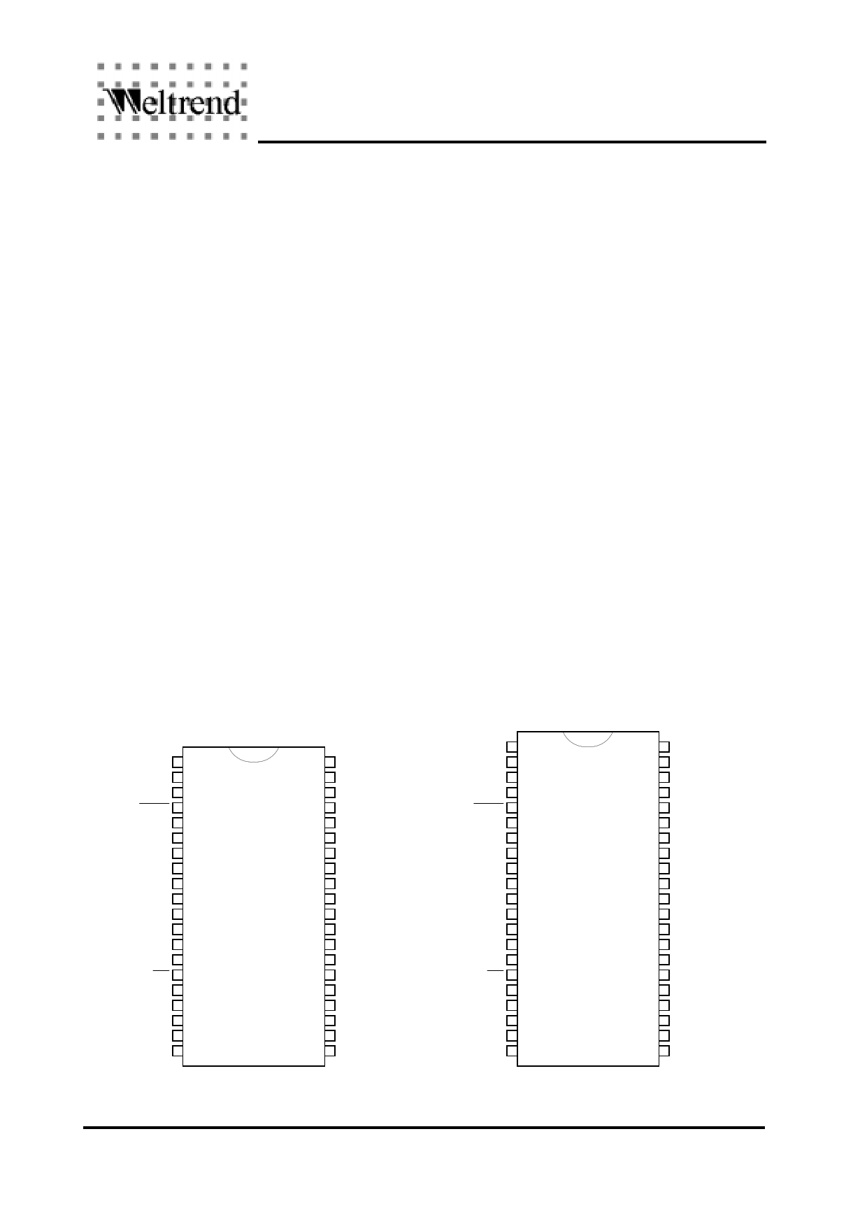
PIN CONFIGURATION
DIP 40-pin
PWM2 1
PWM1 2
PWM0 3
RESET 4
VDD 5
GND 6
OSCO 7
OSCI 8 WT6132
PB5/SDA2 9 WT6124
WT6116PB4/SCL2
PB3/PAT
10
11
PB2 12
PB1/HFI 13
PB0/HFO 14
IRQ 15
PC7/SOGIN 16
PC6 17
PC5 18
PC4 19
PC3/AD3 20
40 VIN
39 HIN
38 PWM3
37 PD5/PWM4
36 PD4/PWM5
35 PD3/PWM6
34 PD2/PWM7
33 PD1/HOUT
32 PD0/VOUT
31 PA7/PWM13/CLAMP
30 PA6/PWM12
29 PA5/PWM11
28 PA4/PWM10
27 PA3/PWM9
26 PA2/PWM8
25 PA1/SCL1
24 PA0/SDA1
23 PC0/AD0
22 PC1/AD1
21 PC2/AD2
Shrink DIP 42-pin
PWM2
PWM1
PWM0
RESET
VDD
GND
OSCO
OSCI
PB5/SDA2
PB4/SCL2
PB3/PAT
PB2
PB1/HFI
PB0/HFO
IRQ
PC7/SOGIN
PC6
PC5
PC4
PC3/AD3
1
2
3
4
5
6
7
8
9
10
11
12
13
14
15
16
17
18
19
20
21
42
41 VIN
40 HIN
39 PWM3
38 PD5/PWM4
37 PD4/PWM5
36 PD3/PWM6
35 PD2/PWM7
WT6132 34 PD1/HOUT
WT6124 33 PD0/VOUT
WT6116 32 PA7/PWM13/CLAMP
31 PA6/PWM12
30 PA5/PWM11
29 PA4/PWM10
28 PA3/PWM9
27 PA2/PWM8
26 PA1/SCL1
25 PA0/SDA1
24 PC0/AD0
23 PC1/AD1
22 PC2/AD2
Weltrend Semiconductor, Inc.
Page 2
1 page 
WT6132/WT6124/WT6116
Data Sheet Rev. 1.01
I/O Port
I/O Port A
Pin PA0 and PA1 are shared with DDC interface SDA1 and SCL1 When ENDDC bit is “0”, These two
pins becomes I/O port. If PA0OE bit is set, Pin PA0 is an open-drain output. If PA0OE is cleared, Pin
PA0 is an input pin with no internal pull-up resistor. The operation of PA1 is same as PA0. Fig. 2 Shows
the structure of PA0.
INTERNAL_DATA_BUS
DATA[0]
D Q PA0OE
WRITE_PA_CTRL
RESET
C QN
R
PA0
DATA[0]
D Q PA0
WRITE_PA_DATA C QN
R
RESET
READ_PA_DATA
DATA[0]
Fig.2 Structure of PA0 and PA1
Pin PA2 to PA6 are shared with PWM output. When corresponding EPWMx bit is “0”, the pin is I/O port.
If PAxOE bit is set, it is a push-pull type output. If PAxOE bit is cleared, it is an input pin with internal
pull-up resistor.
Pin PA7 is shared with PWM13 output and clamp pulse output. When both EPWM13 bit and ENCLP bit
are “0”, this pin becomes I/O port. If PA7OE bit is set, it is a push-pull type output. If PA7OE bit is cleared,
it is an input pin with internal pull-up resistor.
INTERNAL_DATA_BUS
DATA[2]
D Q PA2OE
WRITE_PA_CTRL
RESET
C QN
R
PA2
DATA[2]
D Q PA2
WRITE_PA_DATA C QN
R
RESET
READ_PA_DATA
DATA[2]
Fig.3 Structure of PA2
Weltrend Semiconductor, Inc.
Page 6
5 Page 
WT6132/WT6124/WT6116
Data Sheet Rev. 1.01
Composite Sync Signal Separator
Composite sync signal separator extract Vsync signal from HIN or SOGIN input pin by filtering pulses
which is less than 6us. The output Vsync signal will be widened about 5.5~6.5us. The output Hsync will
be replaced by 2us pulse during Vsync pulse.
The composite sync signal separator can handle H+V and H exclusive OR V signals. Fig.5 shows the
timing relationship of the extracted H and V sync signals.
If Hsync output do not want to insert pseudo H pulses (EXTRHS signal) during Vsync pulse, set BYPASS
bit can let HOUT pin output waveform same as Hsync input (Note: polarity can be controlled by HOPOL
bit).
Hsync
Vsync
H+V
H XOR V
EXTRHS
EXTRVS
Bypass H pulse
Hsync
Insert H pulse
2us 2us
Bypass H pulse
5.5~6.5us
Vsync
H EORV
EXTRHS
EXTRVS
Bypass H pulse
Insert H pulse
2us 2us
Bypass H pulse
5.5~6.5us
Fig. 6 Timing relationship of composite sync signal separator
Weltrend Semiconductor, Inc.
Page 12
11 Page | ||
| Páginas | Total 30 Páginas | |
| PDF Descargar | [ Datasheet WT6116.PDF ] | |
Hoja de datos destacado
| Número de pieza | Descripción | Fabricantes |
| WT6116 | microcontroller for digital controlled monitor | ETC |
| Número de pieza | Descripción | Fabricantes |
| SLA6805M | High Voltage 3 phase Motor Driver IC. |
Sanken |
| SDC1742 | 12- and 14-Bit Hybrid Synchro / Resolver-to-Digital Converters. |
Analog Devices |
|
DataSheet.es es una pagina web que funciona como un repositorio de manuales o hoja de datos de muchos de los productos más populares, |
| DataSheet.es | 2020 | Privacy Policy | Contacto | Buscar |