|
|
|
PDF 74LCXH16374G Data sheet ( Hoja de datos )
| Número de pieza | 74LCXH16374G | |
| Descripción | Low Voltage 16-Bit D-Type Flip-Flop with Bushold | |
| Fabricantes | Fairchild Semiconductor | |
| Logotipo | ||
Hay una vista previa y un enlace de descarga de 74LCXH16374G (archivo pdf) en la parte inferior de esta página. Total 10 Páginas | ||
|
No Preview Available !
February 2001
Revised June 2002
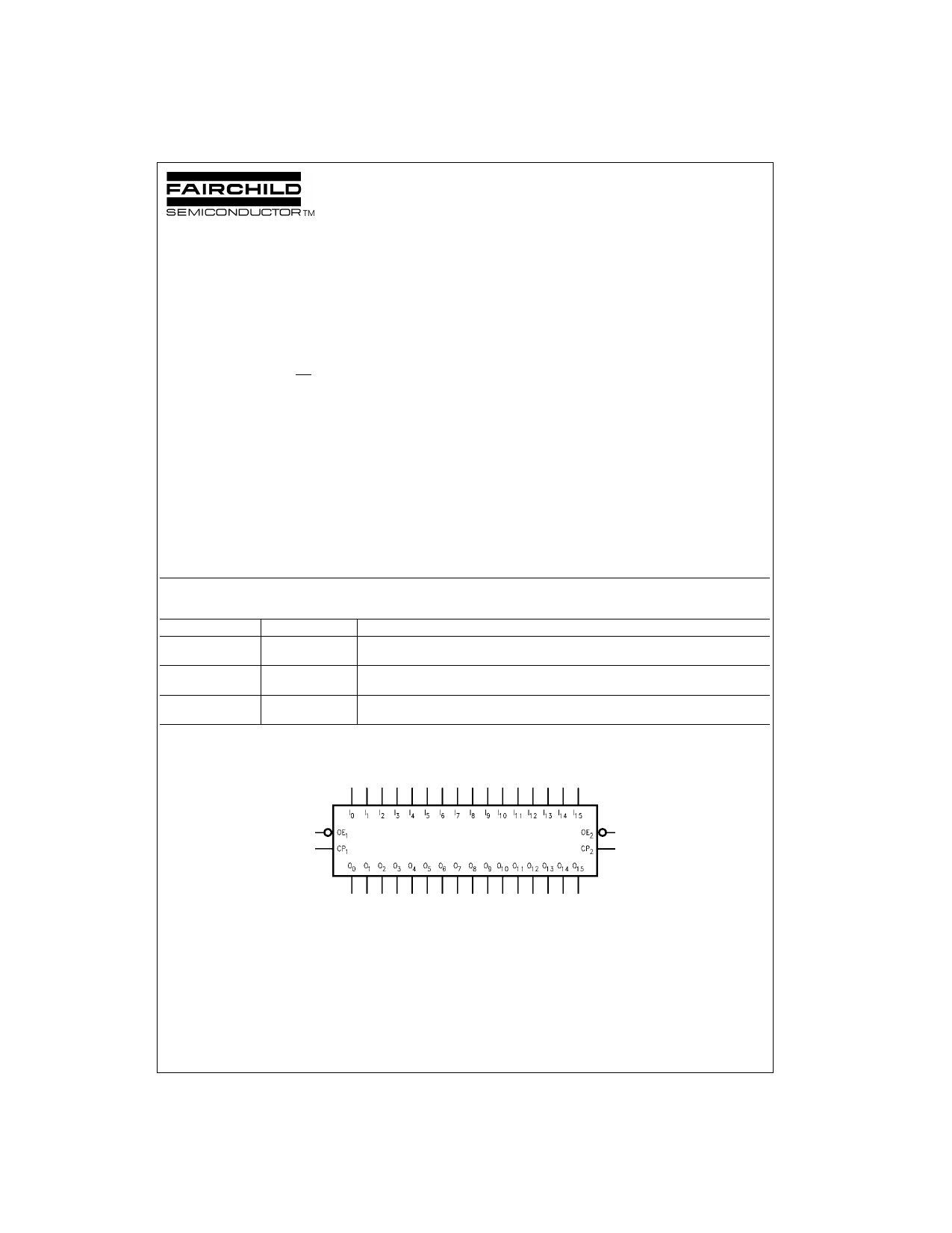
74LCXH16374
Low Voltage 16-Bit D-Type Flip-Flop with Bushold
General Description
The LCXH16374 contains sixteen non-inverting D-type flip-
flops with 3-STATE outputs and is intended for bus oriented
applications. The device is byte controlled. A buffered clock
(CP) and Output Enable (OE) are common to each byte
and can be shorted together for full 16-bit operation.
The LCXH16374 is designed for low voltage (2.5V or 3.3V)
VCC applications.
The LCXH16374 is fabricated with an advanced CMOS
technology to achieve high speed operation while maintain-
ing CMOS low power dissipation.
The LCXH16374 data inputs include active bushold cir-
cuitry, eliminating the need for external pull-up resistors to
hold unused or floating data inputs at a valid logic level.
Features
s 5V tolerant control inputs and outputs
s 2.3V–3.6V VCC specifications provided
s 6.2 ns tPD max (VCC = 3.3V), 20 µA ICC max
s Bushold on inputs eliminating the need for external
pull-up/pull-down resistors
s Power down high impedance outputs
s ±24 mA output drive (VCC = 3.0V)
s Implements patented noise/EMI reduction circuitry
s Latch-up performance exceeds 500 mA
s ESD performance:
Human body model > 2000V
Machine model > 200V
s Also packaged in plastic Fine-Pitch Ball Grid Array
(FBGA)
Ordering Code:
Order Number Package Number
Package Description
74LCXH16374G
(Note 1)(Note 3)
BGA54A
54-Ball Fine-Pitch Ball Grid Array (FBGA), JEDEC MO-205, 5.5mm Wide
74LCXH16374MEA
(Note 2)
MS48A
48-Lead Small Shrink Outline Package (SSOP), JEDEC MO-118, 0.300" Wide
74LCXH16374MTD
(Note 2)
MTD48
48-Lead Thin Shrink Small Outline Package (TSSOP), JEDEC MO-153, 6.1mm Wide
Note 1: Ordering code “G” indicates Trays.
Note 2: Devices also available in Tape and Reel. Specify by appending the suffix letter “X” to the ordering code.
Logic Symbol
GTO is a trademark of Fairchild Semiconductor Corporation.
© 2002 Fairchild Semiconductor Corporation DS500441
www.fairchildsemi.com
1 page 
DC Electrical Characteristics (Continued)
Symbol
Parameter
Conditions
II(HOLD)
Bushold Input Minimum
Drive Hold Current
II(OD)
Bushold Input Over-Drive
Current to Change State
VIN = 0.7V
VIN = 1.7V
VIN = 0.8V
VIN = 2.0V
(Note 7)
(Note 8)
(Note 7)
(Note 8)
IOZ 3-STATE Output Leakage
IOFF Power-Off Leakage Current
ICC Quiescent Supply Current
∆ICC
Increase in ICC per Input
Note 6: Outputs disabled or 3-STATE only.
0 ≤ VO ≤ 5.5V
VO = VCC
VI = VCC or GND
3.6V ≤ VO ≤ 5.5V (Note 6)
VIH = VCC −0.6V
Note 7: An external driver must source at least the specified current to switch from LOW-to-HIGH.
Note 8: An external driver must sink at least the specified current to switch from HIGH-to-LOW.
VCC
(V)
2.3
3.0
2.7
3.6
2.3 − 3.6
0
2.3 − 3.6
2.3 − 3.6
2.3 − 3.6
TA = −40°C to +85°C
Min Max
45
−45
75
−75
300
−300
450
−450
±5.0
10
20
±20
500
Units
µA
µA
µA
µA
µA
µA
AC Electrical Characteristics
TA = −40° to +85°C, RL = 500Ω
Symbol
Parameter
VCC = 3.3V ± 0.3V
CL = 50 pF
VCC = 2.7V
CL = 50 pF
VCC = 2.5V ± 0.2V
CL = 30 pF
Units
Min Max Min Max Min Max
fMAX
Maximum Clock Frequency
170
MHz
tPHL Propagation Delay
tPLH
CP to On
1.5 6.2 1.5 6.5 1.5 7.4
1.5 6.2 1.5 6.5 1.5 7.4
ns
tPZL
tPZH
Output Enable time
1.5 6.1 1.5 6.3 1.5 7.9
1.5 6.1 1.5 6.3 1.5 7.9
ns
tPLZ
tPHZ
Output Disable Time
1.5 6.0 1.5 6.2 1.5 7.2
1.5 6.0 1.5 6.2 1.5 7.2
ns
tS Setup Time
2.5 2.5 3.0
ns
tH Hold Time
1.5 1.5 2.0
ns
tW Pulse Width
3.0 3.0 3.5
ns
tOSHL
tOSLH
Output to Output Skew (Note 9)
1.0
1.0
ns
Note 9: Skew is defined as the absolute value of the differences between the actual propagation delay for any two separate outputs of the same device. The
specification applies to any outputs switching in the same direction, either HIGH-to-LOW (tOSHL) or LOW-to-HIGH (tOSLH). Parameter guaranteed by design.
Dynamic Switching Characteristics
Symbol
Parameter
VOLP
Quiet Output Dynamic Peak VOL
VOLV
Quiet Output Dynamic Valley VOL
Capacitance
Conditions
CL = 50 pF, VIH = 3.3V, VIL = 0V
CL = 30 pF, VIH = 2.5V, VIL = 0V
CL = 50 pF, VIH = 3.3V, VIL = 0V
CL = 30 pF, VIH = 2.5V, VIL = 0V
VCC
TA = 25°C
Units
(V) Typical
3.3 0.8
2.5 0.6
V
3.3 −0.8
2.5 0.6
V
Symbol
CIN
COUT
CPD
Parameter
Input Capacitance
Output Capacitance
Power Dissipation Capacitance
Conditions
VCC = Open, VI = 0V or VCC
VCC = 3.3V, VI = 0V or VCC
VCC = 3.3V, VI = 0V or VCC, f = 10 MHz
Typical
7
8
20
Units
pF
pF
pF
5 www.fairchildsemi.com
5 Page | ||
| Páginas | Total 10 Páginas | |
| PDF Descargar | [ Datasheet 74LCXH16374G.PDF ] | |
Hoja de datos destacado
| Número de pieza | Descripción | Fabricantes |
| 74LCXH16374 | Low Voltage 16-Bit D-Type Flip-Flop with Bushold | Fairchild Semiconductor |
| 74LCXH16374G | Low Voltage 16-Bit D-Type Flip-Flop with Bushold | Fairchild Semiconductor |
| 74LCXH16374MEA | Low Voltage 16-Bit D-Type Flip-Flop with Bushold | Fairchild Semiconductor |
| 74LCXH16374MTD | Low Voltage 16-Bit D-Type Flip-Flop with Bushold | Fairchild Semiconductor |
| Número de pieza | Descripción | Fabricantes |
| SLA6805M | High Voltage 3 phase Motor Driver IC. |
Sanken |
| SDC1742 | 12- and 14-Bit Hybrid Synchro / Resolver-to-Digital Converters. |
Analog Devices |
|
DataSheet.es es una pagina web que funciona como un repositorio de manuales o hoja de datos de muchos de los productos más populares, |
| DataSheet.es | 2020 | Privacy Policy | Contacto | Buscar |