|
|
PDF TDA1572T Data sheet ( Hoja de datos )
| Número de pieza | TDA1572T | |
| Descripción | AM receiver | |
| Fabricantes | NXP Semiconductors | |
| Logotipo | ||
Hay una vista previa y un enlace de descarga de TDA1572T (archivo pdf) en la parte inferior de esta página. Total 20 Páginas | ||
|
No Preview Available !
INTEGRATED CIRCUITS
DATA SHEET
TDA1572T
AM receiver
Product specification
File under Integrated Circuits, IC01
May 1992
1 page 
Philips Semiconductors
AM receiver
Product specification
TDA1572T
FUNCTIONAL DESCRIPTION
Gain-controlled RF stage and mixer
The differential amplifier in the RF stage employs an AGC negative feedback network to provide a wide dynamic range.
Very good cross-modulation behaviour is achieved by AGC delays at the various signal stages. Large signals are
handled with low distortion and the (S + N)/N ratio of small signals is improved. Low noise working is achieved in the
differential amplifier by using transistors with low base resistance.
A double balanced mixer provides the IF output signal to pin 1.
Oscillator
The differential amplifier oscillator is temperature compensated and is suitable for simple coil connection. The oscillator
is voltage-controlled and has little distortion or spurious radiation. It is specially suitable for electronic tuning using
variable capacitance diodes. Band switching diodes can easily be applied using the stabilized voltage V15-20. An extra
buffered oscillator output (pin 14) is available for driving a synthesizer. If this is not needed, resistor RL(14) can be omitted.
Gain-controlled IF amplifier
This amplifier comprises two cascaded, variable-gain differential amplifier stages coupled by a band-pass filter.
Both stages are gain-controlled by the AGC negative feedback network. The IF output is available at pin 12.
Detector
The full-wave, balanced envelope detector has very low distortion over a wide dynamic range. Residual IF carrier is
blocked from the signal path by an internal low-pass filter.
AF preamplifier
This stage preamplifies the audio frequency output signal. The amplifier output has an emitter follower with a series
resistor which, together with an external capacitor, yields the required low-pass for AF filtering.
AGC amplifier
The AGC amplifier provides a control voltage which is proportional to the carrier amplitude. Second-order filtering of the
AGC voltage achieves signals with very little distortion, even at low audio frequencies. This method of filtering also gives
fast AGC settling time which is advantageous for electronic search tuning. The AGC settling time can be further reduced
by using capacitors of smaller value in the external filter (C16 and C17). The AGC voltage is fed to the RF and IF stages
via suitable AGC delays. The capacitor at pin 7 can be omitted for low-cost applications.
Field strength indicator output
A buffered voltage source provides a high-level field strength output signal which has good linearity for logarithmic input
signals over the whole dynamic range. If the field strength information is not needed, RL(13) can be omitted.
Standby switch
This switch is primarily intended for AM/FM band switching. During standby mode the oscillator, mixer and AF
preamplifier are switched off.
Short-circuit protection
All pins have short-circuit protection to ground.
May 1992
5
5 Page 
Philips Semiconductors
AM receiver
Product specification
TDA1572T
SYMBOL
PARAMETER
MIN.
TYP.
MAX.
UNIT
Unwanted signals
Suppression of IF whistles at
Vi = 15 µV; m = 0% related to AF signal
of m = 30%
α2IF at fi ≈ 2 × fIF
α3IF at fi ≈ 3 × fIF
IF suppression at RF input;
− 37 − dB
− 44 − dB
αIF for symmetrical input
αIF for asymmetrical input
Residual oscillator signal at mixer output;
− 40 − dB
− 40 − dB
I1(osc)
I1(2osc)
at fosc
at 2 × fosc
− 1 − µA
− 1.1 − µA
Note
1. AF signals at the IF output will be suppressed by a coupling capacitor to the demodulator and by full wave-detection
in the demodulator.
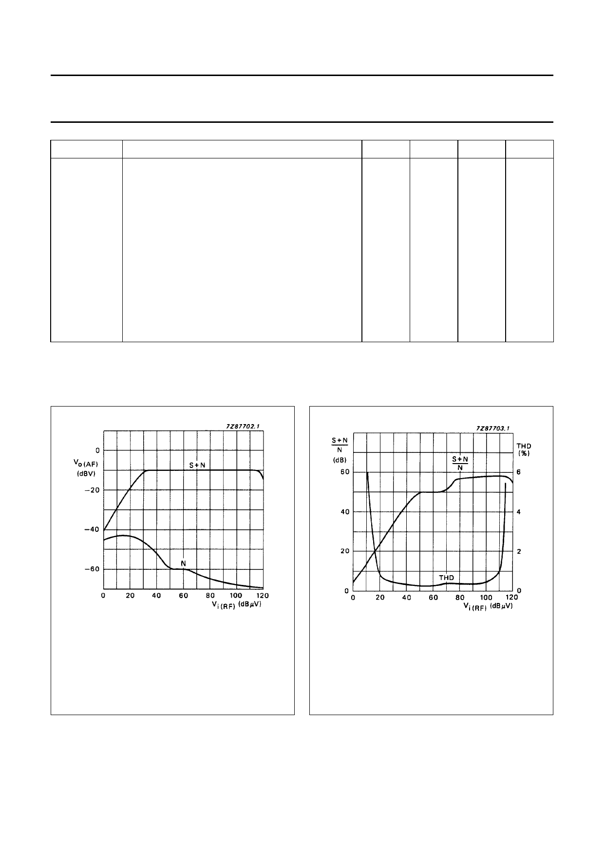
Fig.3 AF output as a function of RF input in the
circuit of Fig.1; fi = 1 MHz; fm = 400 Hz;
m = 30%.
Fig.4
Total harmonic distortion and (S + N)/N as
functions of RF input in the circuit of Fig.1;
m = 30% for (S + N)/N curve and m = 80%
for THD curve.
May 1992
11
11 Page | ||
| Páginas | Total 20 Páginas | |
| PDF Descargar | [ Datasheet TDA1572T.PDF ] | |
Hoja de datos destacado
| Número de pieza | Descripción | Fabricantes |
| TDA1572 | AM receiver circuit | NXP Semiconductors |
| TDA1572T | AM receiver | NXP Semiconductors |
| Número de pieza | Descripción | Fabricantes |
| SLA6805M | High Voltage 3 phase Motor Driver IC. |
Sanken |
| SDC1742 | 12- and 14-Bit Hybrid Synchro / Resolver-to-Digital Converters. |
Analog Devices |
|
DataSheet.es es una pagina web que funciona como un repositorio de manuales o hoja de datos de muchos de los productos más populares, |
| DataSheet.es | 2020 | Privacy Policy | Contacto | Buscar |
