|
|
|
PDF M5M4V4S40CTP-12 Data sheet ( Hoja de datos )
| Número de pieza | M5M4V4S40CTP-12 | |
| Descripción | 4M (2-BANK x 131072-WORD x 16-BIT) Synchronous DRAM | |
| Fabricantes | Mitsubishi | |
| Logotipo | ||
Hay una vista previa y un enlace de descarga de M5M4V4S40CTP-12 (archivo pdf) en la parte inferior de esta página. Total 30 Páginas | ||
|
No Preview Available !
SDRAM (Rev. 0.3)
Feb ‘97 Preliminary
MITSUBISHI LSIs
M5M4V4S40CTP-12, -15
4M (2-BANK x 131072-WORD x 16-BIT) Synchronous DRAM
PRELIMINARY
Some of contents are described for general products
and are subject to change without notice.
DESCRIPTION
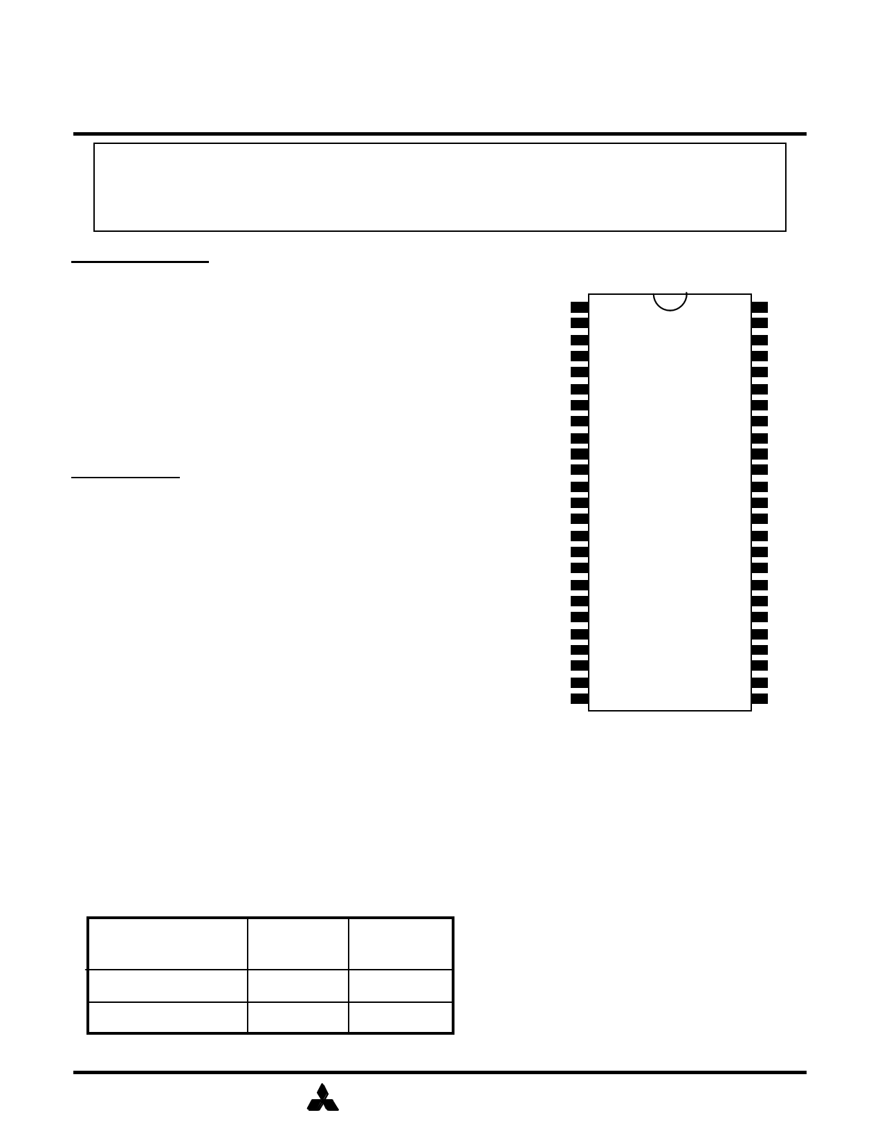
PIN CONFIGURATION
The M5M4V4S40CTP is a 2-bank x 131,072-word x 16-bit
(TOP VIEW)
Synchronous DRAM, with LVTTL interface. All inputs and Vdd
outputs are referenced to the rising edge of CLK. The
DQ0
1
2
50 Vss
49 DQ15
M5M4V4S40CTP achieves very high speed data rates up to DQ1
83MHz, and is suitable for main memory or graphic memory
VssQ
DQ2
in computer systems.
DQ3
3
4
5
6
48 DQ14
47 VssQ
46 DQ13
45 DQ12
VddQ 7
44 VddQ
DQ4
8
43 DQ11
FEATURES
DQ5
VssQ
DQ6
9
10
11
42 DQ10
41 VssQ
40 DQ9
- Single 3.3v±0.3v power supply
- Clock frequency 83MHz / 67MHz
DQ7
VddQ
DQML
12
13
14
39 DQ8
38 VddQ
37 NC
- Fully synchronous operation referenced to clock rising edge /WE 15
- Dual bank operation controlled by BA(Bank Address)
- /CAS latency- 1/2/3 (programmable)
/CAS
/RAS
/CS
16
17
18
- Burst length- 1/2/4/8/FP (programmable)
BA 19
36 DQMU
35 CLK
34 CKE
33 NC
32 NC
- Sequential and interleave burst (programmable)
- Byte control by DQMU and DQML
- Random column access
- Auto precharge / All bank precharge controlled by A8
- Auto and self refresh
A8 20
A0 21
A1 22
A2 23
A3 24
Vdd 25
31 NC
30 A7
29 A6
28 A5
27 A4
26 Vss
- 1024 refresh cycles /16.4ms
- LVTTL Interface
- 400-mil, 50-pin Thin Small Outline Package
(TSOP II) with 0.8mm lead pitch
CLK
CKE
/CS
/RAS
: Master Clock
: Clock Enable
: Chip Select
: Row Address Strobe
/CAS
: Column Address Strobe
/WE : Write Enable
DQ0-15
: Data I/O
DQMU
: Upper Output Disable/ Write Mask
DQML
: Lower Output Disable/ Write Mask
A0-8
: Address Input
BA : Bank Address
Max.
CLK Access
Frequency
Time
Vdd
VddQ
Vss
: Power Supply
: Power Supply for Output
: Ground
M5M4V4S40CTP-12
83MHz
8ns
VssQ
: Ground for Output
M5M4V4S40CTP-15
67MHz
9ns
MITSUBISHI ELECTRIC
1
1 page 
SDRAM (Rev. 0.3)
Feb ‘97 Preliminary
MITSUBISHI LSIs
M5M4V4S40CTP-12, -15
4M (2-BANK x 131072-WORD x 16-BIT) Synchronous DRAM
COMMAND TRUTH TABLE
COMMAND
Deselect
No Operation
Row Address Entry &
Bank Activate
Single Bank Precharge
Precharge All Banks
Column Address Entry
& Write
MNEMONIC
DESEL
NOP
ACT
PRE
PREA
WRITE
CKE
n-1
H
H
H
H
H
H
CKE
n
X
X
X
X
X
X
/CS /RAS /CAS /WE
HX X X
L HHH
L LHH
L LH L
L LH L
LH L L
Column Address Entry
& Write with Auto-
WRITEA H X L H L L
Precharge
Column Address Entry
& Read
Column Address Entry
& Read with Auto-
Precharge
READ
READA
HX LH LH
HX LH LH
Auto-Refresh
Self-Refresh Entry
Self-Refresh Exit
Burst Terminate
Mode Register Set
REFA
REFS
REFSX
TBST
MRS
HH L L LH
HL LL LH
L HHX X X
LH LHHH
HX LHH L
HX L L L L
BA
X
X
V
V
X
V
V
V
V
X
X
X
X
X
V
A8 A0-7
XX
XX
VV
LX
HX
LV
HV
LV
HV
XX
XX
XX
XX
XX
L V*1
H=High Level, L=Low Level, V=Valid, X=Don’t Care, n=CLK cycle number
NOTE:
1. A7 =0, A0-A6 =Mode Address
MITSUBISHI ELECTRIC
5
5 Page 
SDRAM (Rev. 0.3)
Feb ‘97 Preliminary
MITSUBISHI LSIs
M5M4V4S40CTP-12, -15
4M (2-BANK x 131072-WORD x 16-BIT) Synchronous DRAM
SIMPLIFIED STATE DIAGRAM
SELF
REFRESH
REFS
REFSX
MODE
REGISTER
SET
MRS
IDLE
REFA
AUTO
REFRESH
CKEL
CLK
SUSPEND
CKEH
ACT
CKEL
POWER
DOWN
CKEH
TBST(for Full Page)
WRITE
ROW
ACTIVE
TBST(for Full Page)
READ
WRITE
SUSPEND
CKEL
CKEH
WRITE
WRITEA
READA
READ
WRITE
READ
CKEL
CKEH
READ
SUSPEND
WRITEA
CKEL
WRITEA
SUSPEND
CKEH
WRITEA
WRITEA
READA
PRE
PRE
PRE
READA
READA
CKEL
CKEH
READA
SUSPEND
POWER
APPLIED
POWER
ON
PRE
PRE
CHARGE
MITSUBISHI ELECTRIC
Automatic Sequence
Command Sequence
11
11 Page | ||
| Páginas | Total 30 Páginas | |
| PDF Descargar | [ Datasheet M5M4V4S40CTP-12.PDF ] | |
Hoja de datos destacado
| Número de pieza | Descripción | Fabricantes |
| M5M4V4S40CTP-12 | 4M (2-BANK x 131072-WORD x 16-BIT) Synchronous DRAM | Mitsubishi |
| M5M4V4S40CTP-15 | 4M (2-BANK x 131072-WORD x 16-BIT) Synchronous DRAM | Mitsubishi |
| Número de pieza | Descripción | Fabricantes |
| SLA6805M | High Voltage 3 phase Motor Driver IC. |
Sanken |
| SDC1742 | 12- and 14-Bit Hybrid Synchro / Resolver-to-Digital Converters. |
Analog Devices |
|
DataSheet.es es una pagina web que funciona como un repositorio de manuales o hoja de datos de muchos de los productos más populares, |
| DataSheet.es | 2020 | Privacy Policy | Contacto | Buscar |