|
|
|
PDF MGA87563 Data sheet ( Hoja de datos )
| Número de pieza | MGA87563 | |
| Descripción | 0.5 - 4 GHz 3 V Low Current GaAs MMIC LNA | |
| Fabricantes | Agilent(Hewlett-Packard) | |
| Logotipo | ||
Hay una vista previa y un enlace de descarga de MGA87563 (archivo pdf) en la parte inferior de esta página. Total 8 Páginas | ||
|
No Preview Available !
0.5 – 4 GHz 3 V Low Current
GaAs MMIC LNA
Technical Data
MGA-87563
Features
• Ultra-Miniature Package
• 1.6 dB Min. Noise Figure at
2.4 GHz
• 12.5 dB Gain at 2.4 GHz
• Single +3 V or 5 V Supply,
4.5 mA Current
Applications
• LNA or Gain Stage for PCS,
ISM, Cellular, and GPS
Applications
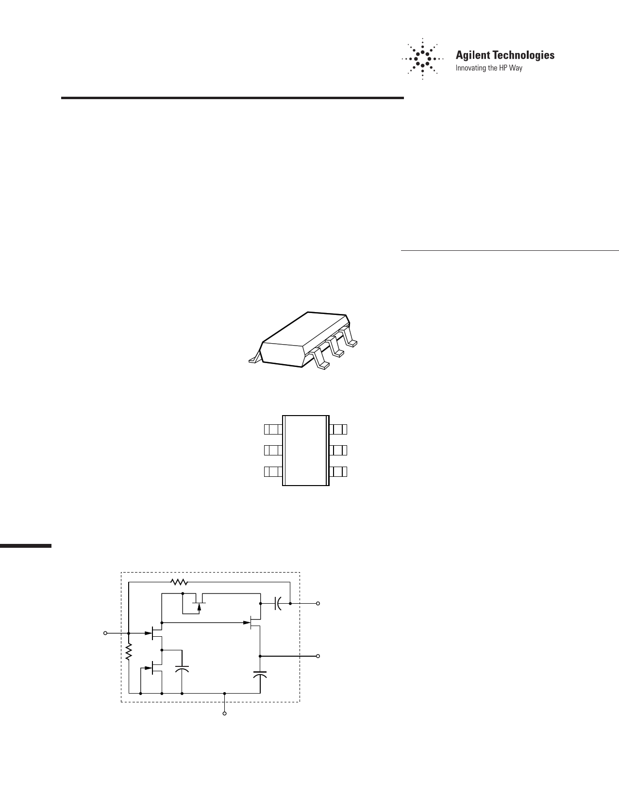
Equivalent Circuit
RF
INPUT
3
Surface Mount SOT-363
(SC-70) Package
Pin Connections and
Package Marking
GND 1
GND 2
INPUT 3
6 OUTPUT
5 GND
4 Vdd
Note:
Package marking provides orientation
and identification.
6
RF
OUTPUT
4
Vdd
Description
Agilent’s MGA-87563 is an
economical, easy-to-use GaAs
MMIC amplifier that offers low
noise and excellent gain for
applications from 0.5 to 4 GHz.
Packaged in an ultra-miniature
SOT-363 package, it requires half
the board space of a SOT-143
package.
With the addition of a simple
shunt-series inductor at the input,
the device is easily matched to
achieve a noise of 1.6 dB at
2.4 GHz. For 2.4 GHz applications
and above, the output is well
matched to 50 Ohms. Below
2 GHz, gain can be increased by
using conjugate matching.
The circuit uses state-of-the-art
PHEMT technology with self-
biasing current sources, a source-
follower interstage, resistive
feedback, and on-chip impedance
matching networks. A patented,
on-chip active bias circuit allows
operation from a single +3 V or
+5 V power supply. Current
consumption is only 4.5 mA,
making this part ideal for battery
powered designs.
GROUND 1, 2, 5
1 page 
5
MGA-87563 Applications
Information
Introduction
The MGA-87563 low noise RF
amplifier is designed to simplify
wireless RF applications in the
0.5 to 4 GHz frequency range. The
MGA-87563 is a two-stage, GaAs
Microwave Monolithic Integrated
Circuit (MMIC) amplifier that
uses feedback to provide
wideband gain. The output is
matched to 50 Ω and the input is
partially matched for optimum
noise figure.
A patented, active bias circuit
makes use of current sources to
“re-use” the drain current in both
stages of gain, thus minimizing
the required supply current and
decreasing sensitivity to varia-
tions in power supply voltage.
Test Circuit
The circuit shown in Figure 10 is
used for 100% RF testing of Noise
Figure and Gain. The input of this
circuit is fixed tuned for a
conjugate power match (maxi-
mum power transfer, or, mini-
mum Input VSWR) at 2 GHz.
Tests in this circuit are used to
guarantee the NFtest and Gtest
parameters shown in the
Electrical Specifications table.
The 4.7 nH inductor, L1 (Coilcraft,
Cary, IL part number series
1008CT-040) placed in series with
Vdd
C1
RF
INPUT
L1
50 Ω 4.7 nH
10 Ω
RF
OUTPUT
50 Ω
the input of the amplifier is all
that is necessary to match the
input to 50 Ω at 2 GHz.
Phase Reference Planes
The positions of the reference
planes used to measure
S-Parameters and to specify Γopt
for the Noise Parameters are
shown in Figure 11. As seen in the
illustration, the reference planes
are located at the extremities of
the package leads.
Biasing
The MGA-87563 is a voltage-
biased device and operates from
a single +3 volt power supply.
With a typical current drain of
only 4.5 mA, the MGA-87563 is
very well suited for use in battery
powered applications. All bias
regulation circuitry is integrated
into the MMIC, eliminating the
need for external DC compo-
nents. RF performance is very
consistent for 3-volt battery
supplies that may range from 2.7
to 3.3 volts, depending on battery
“freshness” or state of charge for
rechargeable batteries. Operation
up to +5 volts is discussed at the
end of the Applications section.
The test circuit in Figure 10
illustrates a suitable method for
bringing bias into the MGA-87563.
The bias connection must be
designed so that it adequately
bypasses the Vdd terminal while
not inadvertently creating any
resonances at frequencies where
the MGA-87563 has gain.
REFERENCE
PLANES
TEST CIRCUIT
The 10 Ω resistor, R1, serves to
“de-Q” any potential resonances
in the bias line that could lead to
low gain, unwanted gain varia-
tions or device instability. The
power supply end of R1 is
bypassed to ground with
capacitor C1. The suggested value
for C1 is 100 pF. Significantly
higher values for C1 are not
recommended. Many higher value
chip capacitors (e.g., 1000 pF) are
not of sufficiently high quality at
these frequencies to function well
as a RF bypass without adding
harmful parasitics or self-
resonances.
While the input and output
terminals are internally resistively
grounded, these pins should not
be considered to be current sinks.
Connection of the MGA-87563
amplifier to circuits that are at
ground potential may be made
without the additional cost and
PCB space needed for DC block-
ing capacitors. If the amplifier is
to be cascaded with active circuits
having non-zero voltages present,
the use of series blocking
capacitors is recommended.
Input Matching
The input of the MGA-87563 is
partially matched internally to
50 Ω. The use of a simple input
conjugate matching circuit (such
as shown in Figure 10 for 2 GHz),
will lower the noise figure
considerably. A significant advan-
tage of the MGA-87563’s design is
that the impedance match for NFo
(minimum noise figure) is very
close to a conjugate power
match. This means that a very
low noise figure can be realized
simultaneously with a low input
VSWR. The typical difference
Figure 10. Test Circuit for 2 GHz.
Figure 11. Reference Planes.
5 Page | ||
| Páginas | Total 8 Páginas | |
| PDF Descargar | [ Datasheet MGA87563.PDF ] | |
Hoja de datos destacado
| Número de pieza | Descripción | Fabricantes |
| MGA87563 | 0.5 - 4 GHz 3 V Low Current GaAs MMIC LNA | Agilent(Hewlett-Packard) |
| Número de pieza | Descripción | Fabricantes |
| SLA6805M | High Voltage 3 phase Motor Driver IC. |
Sanken |
| SDC1742 | 12- and 14-Bit Hybrid Synchro / Resolver-to-Digital Converters. |
Analog Devices |
|
DataSheet.es es una pagina web que funciona como un repositorio de manuales o hoja de datos de muchos de los productos más populares, |
| DataSheet.es | 2020 | Privacy Policy | Contacto | Buscar |