|
|
|
PDF AT88RF256-12 Data sheet ( Hoja de datos )
| Número de pieza | AT88RF256-12 | |
| Descripción | 125 kHz RFID Chip for Cards and Tags | |
| Fabricantes | ATMEL Corporation | |
| Logotipo | ||
Hay una vista previa y un enlace de descarga de AT88RF256-12 (archivo pdf) en la parte inferior de esta página. Total 12 Páginas | ||
|
No Preview Available !
Features
• 125 kHz RFID Chip for Cards and Tags
• 256 Read/Write EEPROM Bits, Divided into Eight Pages of 32 Bits
• Password and Write Lock Protection
• Programmable Send and Receive Protocols
• Support for Multiple Tags (Anti-collision)
• Integrated 150 pF Tuning Capacitor
• ID Length Programmable from 4 - 19 Bytes
• Optional Start and Stop Bits
• Bit Reception Rate of 32 to 4096 Clocks/Bit
• Bit Transmission Rate of 16 to 1024 Clocks/Bit
• Unique Serial Number
• -40° to +85°C Temperature Range
Description
The AT88RF256 is an RFID (radio frequency identification) chip designed to work on
the industry-standard carrier frequency of 125 kHz. Applications include access
control, asset identification, industrial tagging, animal identification and other
applications where modest security capabilities are necessary. Security features
include locking of sensitive information to prevent tampering, optional passwords to
prevent unauthorized access and unique serial numbers locked into the chip by Atmel.
(continued)
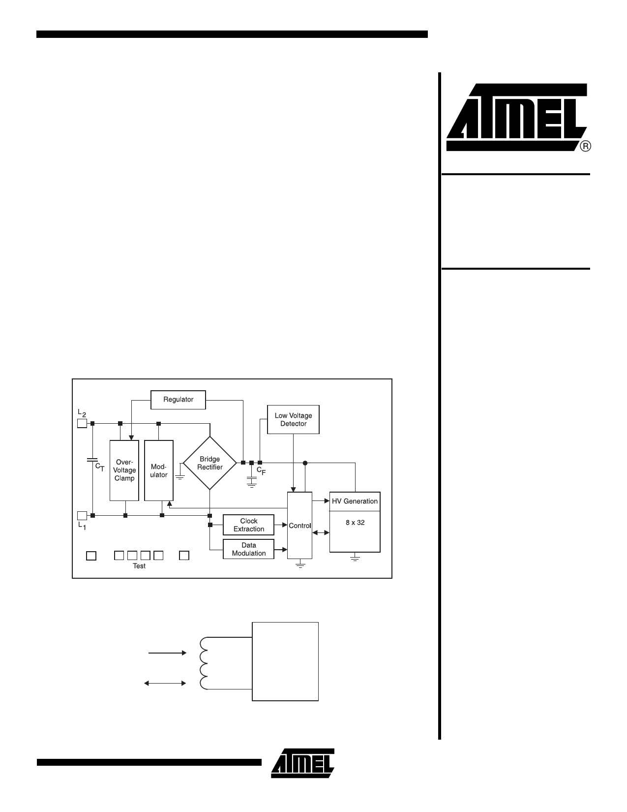
Block Diagram
125 kHz RFID
Transponder
Chip
AT88RF256-12
Preliminary
VSS
VDD
EEPROM
Typical Operating Configuration
External Coil
RF Power
Data
L2
AT88RF256-12
L1
Typical Coil Inductance @125 kHz is ~10.1 mH
Rev. 1684A–07/00
1
1 page 
AT88RF256-12
Data Transmission
The bit rate for data transmitted by the chip, either during
the ID frame or in response to a command, is determined
by the TCLK_GEN bits in the options page. The chip sup-
ports multiples of 16 carrier cycles per bit in the range of 16
to 1024 cycles/bit. All transmission options are amplitude
modulated, using a resistive load across the coil.
The protocol for transmitted data is controlled by three
option fields; ENCODE, INV_ENC and MODULATE. These
fields configure two units that can be connected in a series
or individually bypassed to provide various combinations.
The first stage (the data encoder) implements Manchester
(BiPhase) or Miller data encoding to insert edges into the
data stream. The first stage can be bypassed, permitting
the NRZ data from the EEPROM to go to the second stage
unaltered. This is controlled by the ENCODE option field. If
the inverter is not enabled (INV_ENC) and the modulator
block is bypassed, then a 1 output of the encoder block will
cause the load (modulation device) to be placed across the
coil.
The second stage (the modulation control block) supports
subcarrier and/or PSK schemes, or can be bypassed for
ASK (AM) schemes. For subcarrier and PSK options, the
high-frequency subcarrier is fixed at 62.5 kHz. This block is
controlled by the MODULATE option field.
There is an optional inverter that can be connected
between the first and second stages controlled by
INV_ENC. This option inverts the start and stop bits (if
enabled) so that their true sense becomes the inverse of
that specified by the STOP_1 option bit.
The various encoding and modulation schemes are defined
as follows:
MANCHESTER (sometimes called BiPhase): In the middle
of each bit time there is a transition. If this is a high-to-low,
the data state is a 0, and if low-to-high, the data state is a 1.
MILLER ENCODING: If the data state is a 1, there is a
transition in the middle of the bit time. If the data state is a
0, there is no transition if the previous data bit was a 1.
There is a transition at the beginning of the bit time if the
previous data state is a 0. If the data stream starts with 0
and the data inverter is not enabled, the output of the
encoder will be a 1 during the first bit time.
PHASE SHIFT KEYING (PSK): The modulator is cycled on
and off at a rate of ½ the rate of the carrier frequency.
There is a phase shift with either: a) Every data “1”, sam-
pled at the beginning of each bit time or b) With every data
state change that occurs at either the beginning or middle
of the bit time. This phase shift may occur on either the
high (modulated) or low (unmodulated) phase.
SUBCARRIER: The output of the encoder stage
(Manchester or Miller) gates a subcarrier oscillating at the
rate of ½ the carrier frequency. When the encoder output is
a 1, the carrier will be modulated and when it is a 0, no
modulation will occur.
Although the chip permits all combinations of encoding and
modulation schemes to be selected, some combinations do
not provide useful results. If PSK1 modulation is selected,
then only NRZ encoding will provide useful results since
the chip samples for 1s at the beginning of the bit time only.
If both stages are disabled, it may be difficult to read ID val-
ues composed of all 1s or all 0s.
Data Transmission Circuitry
Input
Data
Data
Encoder
Modulation
Control
To Analog
Modulator
Option Bits
Encode
Inv_enc
62.5 kHz Clock
Modulate
5
5 Page 
Packaging Information (samples only)
8S1, 8-lead, 0.150" Wide, Plastic Gull Wing Small
Outline (JEDEC SOIC)
Dimensions in Inches and (Millimeters)
.020 (.508)
.013 (.330)
PIN 1
.157 (3.99) .244 (6.20)
.150 (3.81) .228 (5.79)
.050 (1.27) BSC
.196 (4.98)
.189 (4.80)
.068 (1.73)
.053 (1.35)
.010 (.254)
.004 (.102)
0
8
REF
.050 (1.27)
.016 (.406)
.010 (.254)
.007 (.203)
AT88RF256-12
11
11 Page | ||
| Páginas | Total 12 Páginas | |
| PDF Descargar | [ Datasheet AT88RF256-12.PDF ] | |
Hoja de datos destacado
| Número de pieza | Descripción | Fabricantes |
| AT88RF256-12 | 125 kHz RFID Chip for Cards and Tags | ATMEL Corporation |
| Número de pieza | Descripción | Fabricantes |
| SLA6805M | High Voltage 3 phase Motor Driver IC. |
Sanken |
| SDC1742 | 12- and 14-Bit Hybrid Synchro / Resolver-to-Digital Converters. |
Analog Devices |
|
DataSheet.es es una pagina web que funciona como un repositorio de manuales o hoja de datos de muchos de los productos más populares, |
| DataSheet.es | 2020 | Privacy Policy | Contacto | Buscar |