|
|
|
PDF 74LVX161284A Data sheet ( Hoja de datos )
| Número de pieza | 74LVX161284A | |
| Descripción | Low Voltage IEEE 161284 Translating Transceiver | |
| Fabricantes | Fairchild Semiconductor | |
| Logotipo | ||
Hay una vista previa y un enlace de descarga de 74LVX161284A (archivo pdf) en la parte inferior de esta página. Total 9 Páginas | ||
|
No Preview Available !
June 1999
Revised July 2000
74LVX161284A
Low Voltage IEEE 161284 Translating Transceiver
General Description
The LVX161284A contains eight bidirectional data buffers
and eleven control/status buffers to implement a full
IEEE 1284 compliant interface. The device supports the
IEEE 1284 standard, with the exception of output slew rate,
and is intended to be used in an Extended Capabilities Port
mode (ECP). The pinout allows for easy connection from
the Peripheral (A-side) to the Host (cable side).
Outputs on the cable side can be configured to be either
open drain or high drive (± 14 mA) and are connected to a
separate power supply pin (VCCcable) to allow these out-
puts to be driven by a higher supply voltage than the
A-side. The pull-up and pull-down series termination resis-
tance of these outputs on the cable side is optimized to
drive an external cable. In addition, all inputs (except HLH)
and outputs on the cable side contain internal pull-up resis-
tors connected to the VCCcable supply to provide proper
termination and pull-ups for open drain mode.
Outputs on the Peripheral side are standard low-drive
CMOS outputs designed to interface with 3V logic. The DIR
input controls data flow on the A1–A8/B1–B8 transceiver
pins.
Features
s Supports IEEE 1284 Level 1 and Level 2 signaling
standards for bidirectional parallel communications
between personal computers and printing peripherals
with the exception of output slew rate
s Translation capability allows outputs on the cable side to
interface with 5V signals
s All inputs have hysteresis to provide noise margin
s B and Y output resistance optimized to drive external
cable
s B and Y outputs in high impedance mode during power
down
s Inputs and outputs on cable side have internal pull-up
resistors
s Flow-through pin configuration allows easy interface
between the “Peripheral and Host”
s Replaces the function of two (2) 74ACT1284 devices
Ordering Code
Order Number
Package
Number
Package Description
74LVX161284AMTD
MTD48
48-Lead Thin Shrink Small Outline Package (TSSOP), JEDEC MO-153, 6.1mm Wide
Device also available in Tape and Reel. Specify by appending suffix letter “X” to the ordering code.
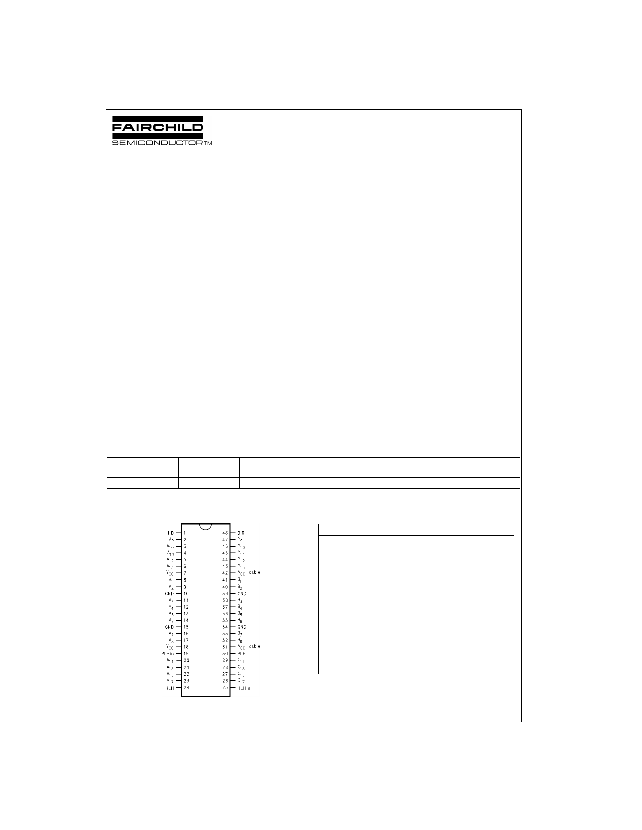
Connection Diagram
Pin Descriptions
Pin Names
Description
HD High Drive Enable Input (Active HIGH)
DIR Direction Control Input
A1–A8
B1–B8
A9–A13
Y9–Y13
A14–A17
C14–C17
PLHIN
PLH
Inputs or Outputs
Inputs or Outputs
Inputs
Outputs
Outputs
Inputs
Peripheral Logic HIGH Input
Peripheral Logic HIGH Output
HLHIN
HLH
Host Logic HIGH Input
Host Logic HIGH Output
© 2000 Fairchild Semiconductor Corporation DS500204
www.fairchildsemi.com
1 page 
AC Electrical Characteristics
TA = −40°C to + 85°C
Symbol
Parameter
VCC = 3.0V–3.6V
VCC—Cable = 4.5V–5.5V
Units
Min Max
tPHL
A1–A8 to B1–B8
1.0 8.5 ns
tPLH
A1–A8 to B1–B8
1.0 8.5 ns
tPHL
B1–B8 to A1–A8
1.0
14.0
ns
tPLH
B1–B8 to A1–A8
1.0
14.0
ns
tPHL
A9–A13 to Y9–Y13
1.0 8.5 ns
tPLH
A9–A13 to Y9–Y13
1.0 8.5 ns
tPHL
C14–C17 to A14–A17
1.0
10.0
ns
tPLH
C14–C17 to A14–A17
1.0
10.0
ns
tSKEW
LH-LH or HL-HL
2.0 ns
tPHL
PLHIN to PLH
1.0 8.5 ns
tPLH
PLHIN to PLH
1.0 8.5 ns
tPHL
HLHIN to HLH
1.0
10.0
ns
tPLH
HLHIN to HLH
1.0
12.0
ns
tPHZ
tPLZ
Output Disable Time
DIR to A1–A8
1.0 10.0
ns
1.0 10.0
tPZH
tPZL
Output Enable Time
DIR to A1–A8
1.0 10.0
ns
1.0 10.0
tPHZ
tPLZ
Output Disable Time
DIR to B1–B8
1.0 13.0
ns
1.0 10.0
tpEN Output Enable Time
HD to B1–B8, Y9–Y13
1.0 8.0 ns
tpDIS
Output Disable Time
HD to B1–B8, Y9–Y13
1.0
12.0
ns
Note 8: tSKEW is measured for common edge output transitions and compares the measured propagation delay for a given path type:
(i) A1–A8 to B1–B8, A9–A13 to Y9–Y13
(ii) B1–B8 to A1–A8
(iii) C14–C17 to A14–A17
Figure
Number
Figure 1
Figure 2
Figure 3
Figure 3
Figure 1
Figure 2
Figure 3
Figure 3
(Note 8)
Figure 1
Figure 2
Figure 3
Figure 3
Figure 4
Figure 5
Figure 6
Figure 2
Figure 2
Capacitance
Symbol
Parameter
Typ Units
Conditions
CIN Input Capacitance
3 pF VCC = 0.0V (HD, DIR, A9–A13, C14–C17, PLHIN and HLHIN)
CI/O (Note 9) I/O Pin Capacitance
5 pF VCC = 3.3V
Note 9: CI/O is measured at frequency = 1 MHz, per MIL-STD-883B, Method 3012
5 www.fairchildsemi.com
5 Page | ||
| Páginas | Total 9 Páginas | |
| PDF Descargar | [ Datasheet 74LVX161284A.PDF ] | |
Hoja de datos destacado
| Número de pieza | Descripción | Fabricantes |
| 74LVX161284 | Low Voltage IEEE 161284 Translating Transceiver | Fairchild Semiconductor |
| 74LVX161284A | Low Voltage IEEE 161284 Translating Transceiver | Fairchild Semiconductor |
| 74LVX161284AMTD | Low Voltage IEEE 161284 Translating Transceiver | Fairchild Semiconductor |
| 74LVX161284MEA | Low Voltage IEEE 161284 Translating Transceiver | Fairchild Semiconductor |
| Número de pieza | Descripción | Fabricantes |
| SLA6805M | High Voltage 3 phase Motor Driver IC. |
Sanken |
| SDC1742 | 12- and 14-Bit Hybrid Synchro / Resolver-to-Digital Converters. |
Analog Devices |
|
DataSheet.es es una pagina web que funciona como un repositorio de manuales o hoja de datos de muchos de los productos más populares, |
| DataSheet.es | 2020 | Privacy Policy | Contacto | Buscar |