|
|
PDF MK2059-01 Data sheet ( Hoja de datos )
| Número de pieza | MK2059-01 | |
| Descripción | VCXO-Based Frame Clock Frequency Translator | |
| Fabricantes | Integrated Circuit Systems | |
| Logotipo |  |
|
Hay una vista previa y un enlace de descarga de MK2059-01 (archivo pdf) en la parte inferior de esta página. Total 10 Páginas | ||
|
No Preview Available !
MK2059-01
VCXO-Based Frame Clock Frequency Translator
Description
The MK2059-01 is a VCXO (Voltage Controlled Crystal
Oscillator) based clock generator that produces
common telecommunications reference frequencies.
The output clock is phase locked to an 8kHz (frame
rate) input reference clock. The MK2059-01 also
provides jitter attenuation. Included in the selection of
output frequencies are these common system clocks:
1.544 MHz (T1)
2.048 (E1)
19.44 MHz (OC-3)
16.384 MHz (8x E1)
This monolithic IC, combined with an external
inexpensive quartz crystal, can be used to replace a
more costly hybrid VCXO retiming module. Through
selection of external loop filter components, the PLL
loop bandwidth and damping factor can be tailored to
meet input clock jitter attenuation requirements. A loop
bandwidth down to the Hz range is possible.
Features
• Generates T1, E1, OC-3 and other common telecom
clock frequencies from an 8kHz frame clock
• Configurable jitter attenuation characterisitics,
excellent for use as a Stratum source de-jitter circuit
• 2:1 Input MUX for input reference clocks
• VCXO-based clock generation offers very low jitter
and phase noise generation
• Output clock is phase and frequency locked to the
selected input reference clock
• Fixed input to output phase relationship
• +115ppm minimum crystal frequency pullability
range, using recommended crystal
• Industrial temperature range
• Low power CMOS technology
• 20 pin SOIC package
• Single 3.3V power supply
Block Diagram
8kHz Ref Input ICLK2
8kHz Ref Input ICLK1
ISEL
1
0
S E L 2 :0
3
IS E T
Phase
D e te c to r
Charge
Pump
Pullable xtal
X1 X2
VDD
VDD 3
VCXO
Output
D iv id e r
Feedback
Divider
CHGP
VIN
GND 4
CLK
MDS 2059-01 B
1
Revision 071001
Integrated Circuit Systems, Inc. q 525 Race Street, San Jose, CA 95126 q tel (408) 295-9800 q www.icst.com
1 page 
MK2059-01
VCXO-Based Frame Clock Frequency Translator
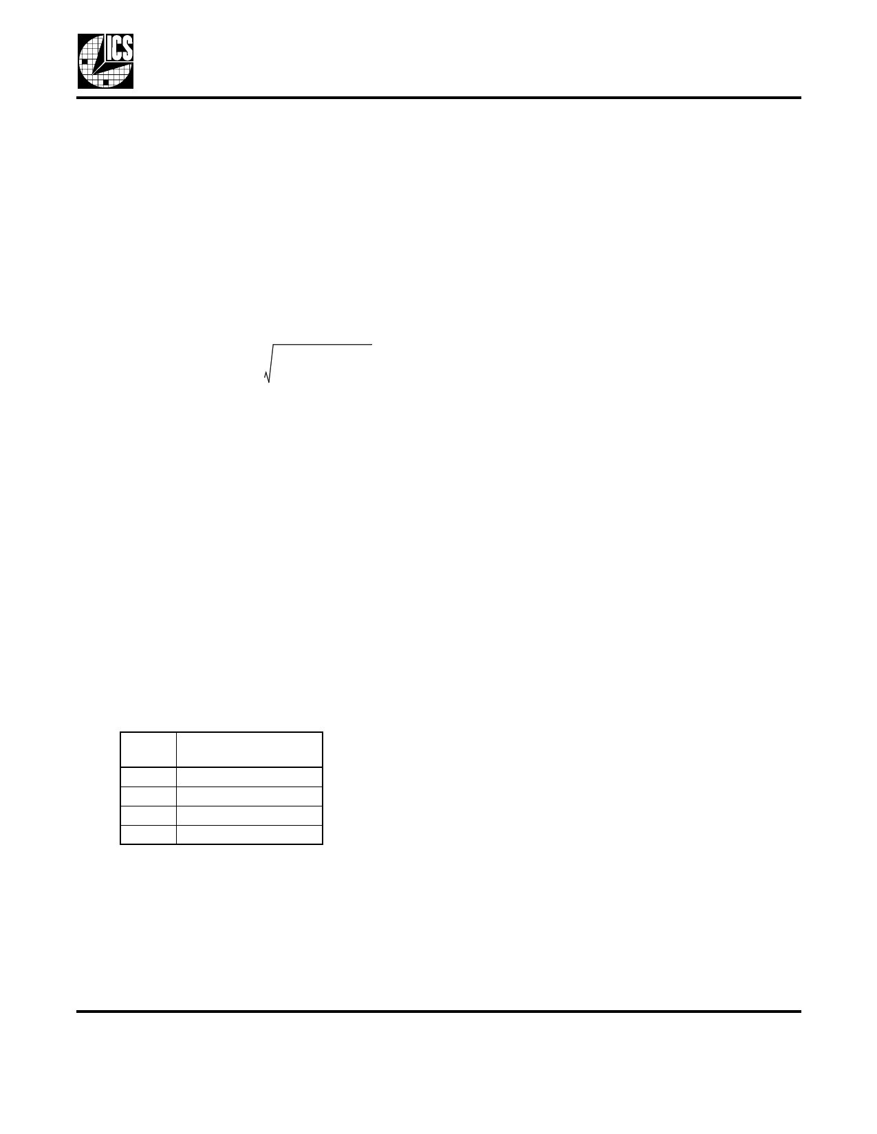
A “normalized” PLL loop bandwidth may be calculated
as follows:
NBW = -R-----Z----×-----I--C-N--P-----×-----5---7----5--
The “normalized” bandwidth equation above does not
take into account the effects of damping factor or the
second pole. However, it does provide a useful
approximation of filter performance.
The loop damping factor is calculated as follows:
Damping Factor = RZ × --6---2----5-----×----I-N-C-----P-----×-----C----1--
Where:
RZ = Value of resistor in loop filter (Ohms)
ICP = Charge pump current (amps)
(refer to Charge Pump Current Table, below)
N = Crystal multiplier shown in the above table
C1 = Value of capacitor C1 in loop filter (Farads)
As a general rule, the following relationship should be
maintained between components C1 and C2 in the loop
filter:
C2
=
C----1-
20
Charge Pump Current Table
RSET
1.4 MΩ
680 kΩ
540 kΩ
120 kΩ
Charge Pump Current
(ICP)
10 µA
20 µA
25 µA
100 µA
1) The loop capacitors should be a low-leakage type to
avoid leakage-induced phase noise. For this reason,
DO NOT use any type of polarized or electrolytic
capacitors.
2) Microphonics (mechanical board vibration) can also
induce output phase noise, especially when the loop
bandwidth is less than 1kHz. For this reason, ceramic
capacitors should have C0G or NP0 dielectric. Avoid
high-K dielectrics like Z5U and X7R. These and some
other ceramics have piezoelectric properties that
convert mechanical vibration into voltage noise that
interferes with VCXO operation.
For larger loop capacitor values such as 0.1 µF or 1 µF,
PPS film types made by Panasonic, or metal poly types
made by Murata or Cornell Dubilier are recommended.
For questions or changes regarding loop filter
characteristics, please contact your sales area FAE, or
ICS MicroClock Applications.
Series Termination Resistor
Clock output traces over one inch should use series
termination. To series terminate a 50Ω trace (a
commonly used trace impedance), place a 33Ω resistor
in series with the clock line, as close to the clock output
pin as possible. The nominal impedance of the clock
output is 20Ω. (The optional series termination resistor
is not shown in the External Component Schematic.)
Decoupling Capacitors
As with any high performance mixed-signal IC, the
MK2059-01 must be isolated from system power
supply noise to perform optimally.
Decoupling capacitors of 0.01µF must be connected
between each VDD and the PCB ground plane. To
further guard against interfering system supply noise,
the MK2059-01 should use one common connection to
the PCB power plane as shown in the diagram on the
next page. The ferrite bead and bulk capacitor help
reduce lower frequency noise in the supply that can
lead to output clock phase modulation.
Special considerations must be made in choosing loop
components C1 and C2:
MDS 2059-01 B
5
Revision 071001
Integrated Circuit Systems, Inc. q 525 Race Street, San Jose, CA 95126 q tel (408) 295-9800 q www.icst.com
5 Page | ||
| Páginas | Total 10 Páginas | |
| PDF Descargar | [ Datasheet MK2059-01.PDF ] | |
Hoja de datos destacado
| Número de pieza | Descripción | Fabricantes |
| MK2059-01 | VCXO-Based Frame Clock Frequency Translator | Integrated Circuit Systems |
| Número de pieza | Descripción | Fabricantes |
| SLA6805M | High Voltage 3 phase Motor Driver IC. |
Sanken |
| SDC1742 | 12- and 14-Bit Hybrid Synchro / Resolver-to-Digital Converters. |
Analog Devices |
|
DataSheet.es es una pagina web que funciona como un repositorio de manuales o hoja de datos de muchos de los productos más populares, |
| DataSheet.es | 2020 | Privacy Policy | Contacto | Buscar |
