|
|
|
PDF MMDF2C02HD Data sheet ( Hoja de datos )
| Número de pieza | MMDF2C02HD | |
| Descripción | COMPLEMENTARY DUAL TMOS POWER FET 2.0 AMPERES 20 VOLTS | |
| Fabricantes | Motorola Semiconductors | |
| Logotipo | ||
Hay una vista previa y un enlace de descarga de MMDF2C02HD (archivo pdf) en la parte inferior de esta página. Total 12 Páginas | ||
|
No Preview Available !
MOTOROLA
SEMICONDUCTOR TECHNICAL DATA
Order this document
by MMDF2C02HD/D
™Designer's Data Sheet
Medium Power Surface Mount Products
Complementary TMOS
Field Effect Transistors
MiniMOS™ devices are an advanced series of power MOSFETs
which utilize Motorola’s High Cell Density HDTMOS process.
These miniature surface mount MOSFETs feature ultra low RDS(on)
and true logic level performance. They are capable of withstanding
high energy in the avalanche and commutation modes and the
drain–to–source diode has a very low reverse recovery time.
MiniMOS devices are designed for use in low voltage, high speed
switching applications where power efficiency is important. Typical
applications are dc–dc converters, and power management in
portable and battery powered products such as computers,
printers, cellular and cordless phones. They can also be used for
low voltage motor controls in mass storage products such as disk
drives and tape drives. The avalanche energy is specified to
eliminate the guesswork in designs where inductive loads are
switched and offer additional safety margin against unexpected
voltage transients.
• Ultra Low RDS(on) Provides Higher Efficiency and Extends
Battery Life
• Logic Level Gate Drive — Can Be Driven by Logic ICs
• Miniature SO–8 Surface Mount Package — Saves Board Space
• Diode Is Characterized for Use In Bridge Circuits
• Diode Exhibits High Speed, With Soft Recovery
• Avalanche Energy Specified
• Mounting Information for SO–8 Package Provided
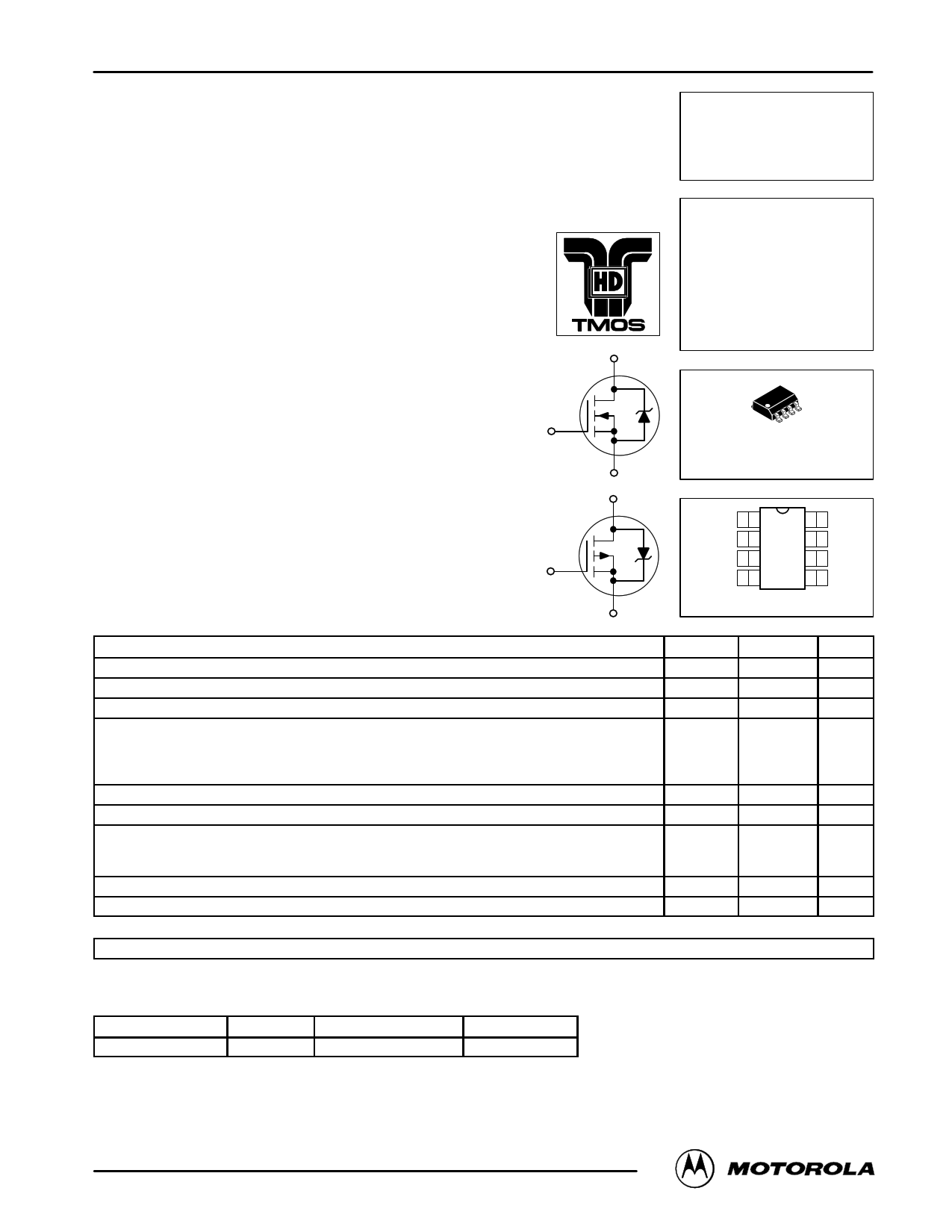
MAXIMUM RATINGS (TJ = 25°C unless otherwise noted)(1)
Rating
D
N–Channel
G
D
P–Channel
G
™
S
S
MMDF2C02HD
Motorola Preferred Device
COMPLEMENTARY
DUAL TMOS POWER FET
2.0 AMPERES
20 VOLTS
RDS(on) = 0.090 OHM
(N–CHANNEL)
RDS(on) = 0.160 OHM
(P–CHANNEL)
CASE 751–05, Style 14
SO–8
N–Source
N–Gate
P–Source
P–Gate
18
27
36
45
Top View
N–Drain
N–Drain
P–Drain
P–Drain
Symbol
Value
Unit
Drain–to–Source Voltage
Gate–to–Source Voltage
Drain–to–Gate Voltage (RGS = 1.0 mΩ)
Drain Current — Continuous
— Pulsed
N–Channel
P–Channel
N–Channel
P–Channel
Operating and Storage Temperature Range
Total Power Dissipation @ TA= 25°C (2)
Single Pulse Drain–to–Source Avalanche Energy — Starting TJ = 25°C
(VDD = 20 V, VGS = 5.0 V, Peak IL = 9.0 A, L = 10 mH, RG = 25 Ω)
(VDD = 20 V, VGS = 5.0 V, Peak IL = 6.0 A, L = 18 mH, RG = 25 Ω)
Thermal Resistance — Junction to Ambient (2)
N–Channel
P–Channel
Maximum Lead Temperature for Soldering, 0.0625″ from case. Time in Solder Bath is 10 seconds.
DEVICE MARKING
VDSS
VGS
VDGR
ID
IDM
TJ, Tstg
PD
EAS
RθJA
TL
20
± 20
20
3.8
3.3
19
20
– 55 to 150
2.0
405
324
62.5
260
Vdc
Vdc
Vdc
A
°C
Watts
mJ
°C/W
°C
D2C02
(1) Negative signs for P–Channel device omitted for clarity.
(2) Mounted on 2” square FR4 board (1” sq. 2 oz. Cu 0.06” thick single sided) with one die operating, 10 sec. max.
ORDERING INFORMATION
Device
Reel Size
Tape Width
Quantity
MMDF2C02HDR2
13″
12 mm embossed tape
2500 units
Designer’s Data for “Worst Case” Conditions — The Designer’s Data Sheet permits the design of most circuits entirely from the information presented. SOA Limit
curves — representing boundaries on device characteristics — are given to facilitate “worst case” design.
HDTMOS and MiniMOS are trademarks of Motorola, Inc. TMOS is a registered trademark of Motorola, Inc.
Thermal Clad is a trademark of the Bergquist Company.
Preferred devices are Motorola recommended choices for future use and best overall value.
REV 5
©MMoottoororolal,aInTc.M19O9S6 Power MOSFET Transistor Device Data
1
1 page 
MMDF2C02HD
TYPICAL ELECTRICAL CHARACTERISTICS
N–Channel
P–Channel
1000
VGS = 0 V
100
VGS = 0 V
TJ = 125°C
100 TJ = 125°C
100°C
25°C
10
10
100°C
1
0 4 8 12 16 20
VDS, DRAIN–TO–SOURCE VOLTAGE (VOLTS)
Figure 6. Drain–To–Source Leakage
Current versus Voltage
1
0 5 10 15 20
VDS, DRAIN–TO–SOURCE VOLTAGE (VOLTS)
Figure 6. Drain–To–Source Leakage
Current versus Voltage
POWER MOSFET SWITCHING
Switching behavior is most easily modeled and predicted
by recognizing that the power MOSFET is charge controlled.
The lengths of various switching intervals (∆t) are deter-
mined by how fast the FET input capacitance can be charged
by current from the generator.
The published capacitance data is difficult to use for calculat-
ing rise and fall because drain–gate capacitance varies
greatly with applied voltage. Accordingly, gate charge data is
used. In most cases, a satisfactory estimate of average input
current (IG(AV)) can be made from a rudimentary analysis of
the drive circuit so that
t = Q/IG(AV)
During the rise and fall time interval when switching a resis-
tive load, VGS remains virtually constant at a level known as
the plateau voltage, VSGP. Therefore, rise and fall times may
be approximated by the following:
tr = Q2 x RG/(VGG – VGSP)
tf = Q2 x RG/VGSP
where
VGG = the gate drive voltage, which varies from zero to VGG
RG = the gate drive resistance
and Q2 and VGSP are read from the gate charge curve.
During the turn–on and turn–off delay times, gate current is
not constant. The simplest calculation uses appropriate val-
ues from the capacitance curves in a standard equation for
voltage change in an RC network. The equations are:
td(on) = RG Ciss In [VGG/(VGG – VGSP)]
td(off) = RG Ciss In (VGG/VGSP)
The capacitance (Ciss) is read from the capacitance curve at
a voltage corresponding to the off–state condition when cal-
culating td(on) and is read at a voltage corresponding to the
on–state when calculating td(off).
At high switching speeds, parasitic circuit elements com-
plicate the analysis. The inductance of the MOSFET source
lead, inside the package and in the circuit wiring which is
common to both the drain and gate current paths, produces a
voltage at the source which reduces the gate drive current.
The voltage is determined by Ldi/dt, but since di/dt is a func-
tion of drain current, the mathematical solution is complex.
The MOSFET output capacitance also complicates the
mathematics. And finally, MOSFETs have finite internal gate
resistance which effectively adds to the resistance of the
driving source, but the internal resistance is difficult to mea-
sure and, consequently, is not specified.
The resistive switching time variation versus gate resis-
tance (Figure 9) shows how typical switching performance is
affected by the parasitic circuit elements. If the parasitics
were not present, the slope of the curves would maintain a
value of unity regardless of the switching speed. The circuit
used to obtain the data is constructed to minimize common
inductance in the drain and gate circuit loops and is believed
readily achievable with board mounted components. Most
power electronic loads are inductive; the data in the figure is
taken with a resistive load, which approximates an optimally
snubbed inductive load. Power MOSFETs may be safely op-
erated into an inductive load; however, snubbing reduces
switching losses.
Motorola TMOS Power MOSFET Transistor Device Data
5
5 Page 
MMDF2C02HD
TYPICAL SOLDER HEATING PROFILE
For any given circuit board, there will be a group of control
settings that will give the desired heat pattern. The operator
must set temperatures for several heating zones and a figure
for belt speed. Taken together, these control settings make up
a heating “profile” for that particular circuit board. On
machines controlled by a computer, the computer remembers
these profiles from one operating session to the next. Figure
16 shows a typical heating profile for use when soldering a
surface mount device to a printed circuit board. This profile will
vary among soldering systems, but it is a good starting point.
Factors that can affect the profile include the type of soldering
system in use, density and types of components on the board,
type of solder used, and the type of board or substrate material
being used. This profile shows temperature versus time. The
line on the graph shows the actual temperature that might be
experienced on the surface of a test board at or near a central
solder joint. The two profiles are based on a high density and
a low density board. The Vitronics SMD310 convection/in-
frared reflow soldering system was used to generate this
profile. The type of solder used was 62/36/2 Tin Lead Silver
with a melting point between 177 –189°C. When this type of
furnace is used for solder reflow work, the circuit boards and
solder joints tend to heat first. The components on the board
are then heated by conduction. The circuit board, because it
has a large surface area, absorbs the thermal energy more
efficiently, then distributes this energy to the components.
Because of this effect, the main body of a component may be
up to 30 degrees cooler than the adjacent solder joints.
200°C
STEP 1
PREHEAT
ZONE 1
“RAMP”
STEP 2
VENT
“SOAK”
STEP 3
HEATING
ZONES 2 & 5
“RAMP”
STEP 4
STEP 5
HEATING HEATING
ZONES 3 & 6 ZONES 4 & 7
“SOAK”
“SPIKE”
DESIRED CURVE FOR HIGH
MASS ASSEMBLIES
160°C
170°C
STEP 6
VENT
STEP 7
COOLING
205° TO 219°C
PEAK AT
SOLDER JOINT
150°C
100°C
150°C
100°C
140°C
SOLDER IS LIQUID FOR
40 TO 80 SECONDS
(DEPENDING ON
MASS OF ASSEMBLY)
DESIRED CURVE FOR LOW
MASS ASSEMBLIES
50°C
TIME (3 TO 7 MINUTES TOTAL)
TMAX
Figure 16. Typical Solder Heating Profile
Motorola TMOS Power MOSFET Transistor Device Data
11
11 Page | ||
| Páginas | Total 12 Páginas | |
| PDF Descargar | [ Datasheet MMDF2C02HD.PDF ] | |
Hoja de datos destacado
| Número de pieza | Descripción | Fabricantes |
| MMDF2C02HD | COMPLEMENTARY DUAL TMOS POWER FET 2.0 AMPERES 20 VOLTS | Motorola Semiconductors |
| MMDF2C02HD | Power MOSFET ( Transistor ) | ON Semiconductor |
| Número de pieza | Descripción | Fabricantes |
| SLA6805M | High Voltage 3 phase Motor Driver IC. |
Sanken |
| SDC1742 | 12- and 14-Bit Hybrid Synchro / Resolver-to-Digital Converters. |
Analog Devices |
|
DataSheet.es es una pagina web que funciona como un repositorio de manuales o hoja de datos de muchos de los productos más populares, |
| DataSheet.es | 2020 | Privacy Policy | Contacto | Buscar |