|
|
|
PDF MMFT107T1 Data sheet ( Hoja de datos )
| Número de pieza | MMFT107T1 | |
| Descripción | MEDIUM POWER TMOS FET 250 mA / 200 VOLTS | |
| Fabricantes | Motorola Semiconductors | |
| Logotipo | ||
Hay una vista previa y un enlace de descarga de MMFT107T1 (archivo pdf) en la parte inferior de esta página. Total 6 Páginas | ||
|
No Preview Available !
MOTOROLA
SEMICONDUCTOR TECHNICAL DATA
Order this document
by MMFT107T1/D
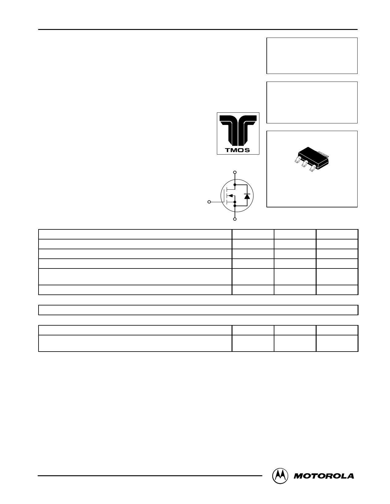
Medium Power Field Effect
Transistor
N–Channel Enhancement–Mode
Silicon Gate TMOS
SOT–223 for Surface Mount
This TMOS medium power field effect transistor is designed for
high speed, low loss power switching applications such as
switching regulators, dc–dc converters, solenoid and relay drivers.
The device is housed in the SOT–223 package which is designed
for medium power surface mount applications.
• Silicon Gate for Fast Switching Speeds
• RDS(on) = 14 Ohm Max
• Low Drive Requirement
• The SOT–223 Package can be soldered using wave or reflow.
The formed leads absorb thermal stress during soldering
eliminating the possibility of damage to the die.
• Available in 12 mm Tape and Reel
Use MMFT107T1 to order the 7 inch/1000 unit reel
Use MMFT107T3 to order the 13 inch/4000 unit reel
1
GATE
®
2,4 DRAIN
MAXIMUM RATINGS (TC = 25°C unless otherwise noted)
Rating
3 SOURCE
Symbol
Drain–to–Source Voltage
Gate–to–Source Voltage — Non–Repetitive
Drain Current
Total Power Dissipation @ TA = 25°C(1)
Derate above 25°C
VDSS
VGS
ID
PD
Operating and Storage Temperature Range
DEVICE MARKING
TJ, Tstg
FT107
THERMAL CHARACTERISTICS
Thermal Resistance — Junction–to–Ambient
Maximum Temperature for Soldering Purposes
Time in Solder Bath
RθJA
TL
1. Device mounted on FR–4 glass epoxy printed circuit using minimum recommended footprint.
MMFT107T1
Motorola Preferred Device
MEDIUM POWER
TMOS FET
250 mA, 200 VOLTS
RDS(on) = 14 OHM MAX
1
2
3
4
CASE 318E–04, STYLE 3
TO–261AA
Value
200
± 20
250
0.8
6.4
– 65 to 150
Unit
Volts
Volts
mAdc
Watts
mW/°C
°C
156 °C/W
260 °C
10 Sec
TMOS is a registered trademark of Motorola, Inc.
Thermal Clad is a trademark of the Bergquist Company
Preferred devices are Motorola recommended choices for future use and best overall value.
REV 3
©MMoototorroollaa, ISncm. 1a9l9l–7Signal Transistors, FETs and Diodes Device Data
1
1 page 
MMFT107T1
SOLDER STENCIL GUIDELINES
Prior to placing surface mount components onto a printed
circuit board, solder paste must be applied to the pads. A
solder stencil is required to screen the optimum amount of
solder paste onto the footprint. The stencil is made of brass
or stainless steel with a typical thickness of 0.008 inches.
The stencil opening size for the SOT-223 package should be
the same as the pad size on the printed circuit board, i.e., a
1:1 registration.
SOLDERING PRECAUTIONS
The melting temperature of solder is higher than the rated
temperature of the device. When the entire device is heated
to a high temperature, failure to complete soldering within a
short time could result in device failure. Therefore, the
following items should always be observed in order to
minimize the thermal stress to which the devices are
subjected.
• Always preheat the device.
• The delta temperature between the preheat and
soldering should be 100°C or less.*
• When preheating and soldering, the temperature of the
leads and the case must not exceed the maximum
temperature ratings as shown on the data sheet. When
using infrared heating with the reflow soldering method,
the difference should be a maximum of 10°C.
• The soldering temperature and time should not exceed
260°C for more than 10 seconds.
• When shifting from preheating to soldering, the
maximum temperature gradient should be 5°C or less.
• After soldering has been completed, the device should
be allowed to cool naturally for at least three minutes.
Gradual cooling should be used as the use of forced
cooling will increase the temperature gradient and result
in latent failure due to mechanical stress.
• Mechanical stress or shock should not be applied during
cooling
* Soldering a device without preheating can cause excessive
thermal shock and stress which can result in damage to the
device.
TYPICAL SOLDER HEATING PROFILE
For any given circuit board, there will be a group of control
settings that will give the desired heat pattern. The operator
must set temperatures for several heating zones, and a
figure for belt speed. Taken together, these control settings
make up a heating “profile” for that particular circuit board.
On machines controlled by a computer, the computer
remembers these profiles from one operating session to the
next. Figure 10 shows a typical heating profile for use when
soldering a surface mount device to a printed circuit board.
This profile will vary among soldering systems but it is a good
starting point. Factors that can affect the profile include the
type of soldering system in use, density and types of
components on the board, type of solder used, and the type
of board or substrate material being used. This profile shows
temperature versus time. The line on the graph shows the
actual temperature that might be experienced on the surface
of a test board at or near a central solder joint. The two
profiles are based on a high density and a low density board.
The Vitronics SMD310 convection/infrared reflow soldering
system was used to generate this profile. The type of solder
used was 62/36/2 Tin Lead Silver with a melting point
between 177 –189°C. When this type of furnace is used for
solder reflow work, the circuit boards and solder joints tend to
heat first. The components on the board are then heated by
conduction. The circuit board, because it has a large surface
area, absorbs the thermal energy more efficiently, then
distributes this energy to the components. Because of this
effect, the main body of a component may be up to 30
degrees cooler than the adjacent solder joints.
200°C
STEP 1 STEP 2 STEP 3
STEP 4
STEP 5 STEP 6 STEP 7
PREHEAT VENT HEATING
HEATING HEATING VENT COOLING
ZONE 1
“RAMP”
“SOAK” ZONES 2 & 5 ZONES 3 & 6 ZONES 4 & 7
“RAMP”
“SOAK”
“SPIKE”
205° TO
219°C
DESIRED CURVE FOR HIGH
170°C
PEAK AT
MASS ASSEMBLIES
160°C
SOLDER
150°C
JOINT
150°C
100°C
100°C
140°C
SOLDER IS LIQUID FOR
40 TO 80 SECONDS
(DEPENDING ON
MASS OF ASSEMBLY)
DESIRED CURVE FOR LOW
MASS ASSEMBLIES
50°C
TIME (3 TO 7 MINUTES TOTAL)
TMAX
Figure 10. Typical Solder Heating Profile
Motorola Small–Signal Transistors, FETs and Diodes Device Data
5
5 Page | ||
| Páginas | Total 6 Páginas | |
| PDF Descargar | [ Datasheet MMFT107T1.PDF ] | |
Hoja de datos destacado
| Número de pieza | Descripción | Fabricantes |
| MMFT107T1 | MEDIUM POWER TMOS FET 250 mA / 200 VOLTS | Motorola Semiconductors |
| MMFT107T1 | Power MOSFET 250 mA / 200 Volts | ON |
| MMFT107T3 | Power MOSFET 250 mA / 200 Volts | ON |
| Número de pieza | Descripción | Fabricantes |
| SLA6805M | High Voltage 3 phase Motor Driver IC. |
Sanken |
| SDC1742 | 12- and 14-Bit Hybrid Synchro / Resolver-to-Digital Converters. |
Analog Devices |
|
DataSheet.es es una pagina web que funciona como un repositorio de manuales o hoja de datos de muchos de los productos más populares, |
| DataSheet.es | 2020 | Privacy Policy | Contacto | Buscar |