|
|
|
PDF N302AP Data sheet ( Hoja de datos )
| Número de pieza | N302AP | |
| Descripción | N-Channel Logic Level PWM Optimized UltraFET Trench Power MOSFETs | |
| Fabricantes | Fairchild | |
| Logotipo | ||
Hay una vista previa y un enlace de descarga de N302AP (archivo pdf) en la parte inferior de esta página. Total 10 Páginas | ||
|
No Preview Available !
January 2002
ISL9N302AP3
N-Channel Logic Level PWM Optimized UltraFET® Trench Power MOSFETs
General Description
This device employs a new advanced trench MOSFET
technology and features low gate charge while maintaining
low on-resistance.
Optimized for switching applications, this device improves
the overall efficiency of DC/DC converters and allows
operation to higher switching frequencies.
Applications
• DC/DC converters
Features
• Fast switching
• rDS(ON) = 0.0019Ω (Typ), VGS = 10V
• rDS(ON) = 0.0027Ω (Typ), VGS = 4.5V
• Qg (Typ) = 110nC, VGS = 5V
• Qgd (Typ) = 31nC
• CISS (Typ) = 11000pF
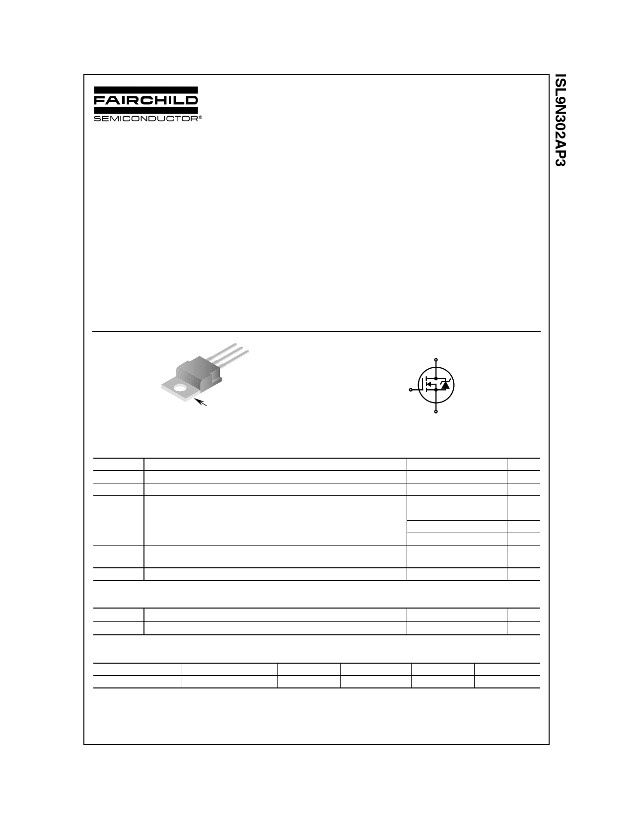
SOURCE
DRAIN
GATE
D
DRAIN
(FLANGE)
TO-220AB
G
MOSFET Maximum Ratings TA = 25°C unless otherwise noted
Symbol
VDSS
VGS
ID
Parameter
Drain to Source Voltage
Gate to Source Voltage
Drain Current
Continuous (TC = 25oC, VGS = 10V)
Continuous (TC = 100oC, VGS = 4.5V)
Pulsed
PD
Power dissipation
Derate above 25oC
TJ, TSTG Operating and Storage Temperature
Thermal Characteristics
RθJC
RθJA
Thermal Resistance Junction to Case TO-220
Thermal Resistance Junction to Ambient TO-220
Package Marking and Ordering Information
Device Marking
N302AP
Device
ISL9N302AP3
Package
TO-220AB
Reel Size
Tube
S
Ratings
30
±20
75
75
Figure 4
345
2.3
-55 to 175
0.43
62
Tape Width
N/A
Units
V
V
A
A
A
W
W/oC
oC
oC/W
oC/W
Quantity
50
©2002 Fairchild Semiconductor Corporation
Rev. B January 2002
1 page 
Typical Characteristic (Continued)
20000
10000
COSS ≅ CDS + CGD
CISS = CGS + CGD
10
VDD = 15V
8
6
CRSS = CGD
1000
VGS = 0V, f = 1MHz
500
0.1
1
10 30
VDS, DRAIN TO SOURCE VOLTAGE (V)
Figure 11. Capacitance vs Drain to Source
Voltage
4
2
0
0
WAVEFORMS IN
DESCENDING ORDER:
ID = 75A
ID = 28A
50 100 150 200 250
Qg, GATE CHARGE (nC)
Figure 12. Gate Charge Waveforms for Constant
Gate Currents
1000
800
VGS = 4.5V, VDD = 15V, ID = 28A
600 tr
tf
400
200
0
0
td(ON)
td(OFF)
10 20 30 40
RGS, GATE TO SOURCE RESISTANCE (Ω)
50
Figure 13. Switching Time vs Gate Resistance
Test Circuits and Waveforms
1400
1200
VGS = 10V, VDD = 15V, ID = 28A
1000
800
600
400
200
0
0
td(OFF)
tf
tr
td(ON)
10 20 30 40 50
RGS, GATE TO SOURCE RESISTANCE (Ω)
Figure 14. Switching Time vs Gate Resistance
VARY tP TO OBTAIN
REQUIRED PEAK IAS
VGS
tP
0V
RG
VDS
L
DUT
+
VDD
-
IAS
0.01Ω
Figure 15. Unclamped Energy Test Circuit
tP
IAS
BVDSS
VDS
VDD
0
tAV
Figure 16. Unclamped Energy Waveforms
©2002 Fairchild Semiconductor Corporation
Rev. B January 2002
5 Page | ||
| Páginas | Total 10 Páginas | |
| PDF Descargar | [ Datasheet N302AP.PDF ] | |
Hoja de datos destacado
| Número de pieza | Descripción | Fabricantes |
| N302AP | N-Channel Logic Level PWM Optimized UltraFET Trench Power MOSFETs | Fairchild |
| N302AS | N-Channel Logic Level PWM Optimized UltraFET Trench Power MOSFETs | Fairchild |
| Número de pieza | Descripción | Fabricantes |
| SLA6805M | High Voltage 3 phase Motor Driver IC. |
Sanken |
| SDC1742 | 12- and 14-Bit Hybrid Synchro / Resolver-to-Digital Converters. |
Analog Devices |
|
DataSheet.es es una pagina web que funciona como un repositorio de manuales o hoja de datos de muchos de los productos más populares, |
| DataSheet.es | 2020 | Privacy Policy | Contacto | Buscar |