|
|
|
PDF OP-184 Data sheet ( Hoja de datos )
| Número de pieza | OP-184 | |
| Descripción | Precision Rail-to-Rail Input & Output Operational Amplifiers | |
| Fabricantes | Analog Devices | |
| Logotipo | ||
Hay una vista previa y un enlace de descarga de OP-184 (archivo pdf) en la parte inferior de esta página. Total 20 Páginas | ||
|
No Preview Available !
a
FEATURES
Single-Supply Operation
Wide Bandwidth: 4 MHz
Low Offset Voltage: 65 V
Unity-Gain Stable
High Slew Rate: 4.0 V/s
Low Noise: 3.9 nV/√Hz
APPLICATIONS
Battery Powered Instrumentation
Power Supply Control and Protection
Telecom
DAC Output Amplifier
ADC Input Buffer
Precision Rail-to-Rail Input & Output
Operational Amplifiers
OP184/OP284/OP484
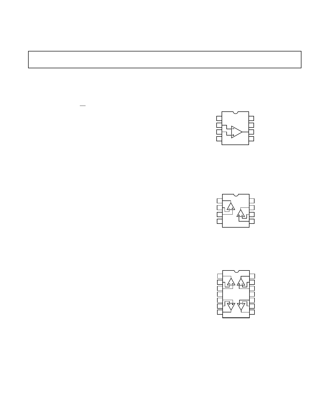
PIN CONFIGURATIONS
8-Lead Epoxy DIP
(P Suffix)
8-Lead SO
(S Suffix)
NULL 1
–IN A 2
+IN A 3
V– 4
OP184
8 NC
7 V+
6 OUT A
5 NULL
NC = NO CONNECT
GENERAL DESCRIPTION
The OP184/OP284/OP484 are single, dual and quad single-
supply, 4 MHz bandwidth amplifiers featuring rail-to-rail inputs
and outputs. They are guaranteed to operate from +3 to +36 (or
± 1.5 to ± 18) volts and will function with a single supply as low
as +1.5 volts.
These amplifiers are superb for single supply applications re-
quiring both ac and precision dc performance. The combination
of bandwidth, low noise and precision makes the OP184/OP284/
OP484 useful in a wide variety of applications, including filters
and instrumentation.
Other applications for these amplifiers include portable telecom
equipment, power supply control and protection, and as amplifi-
ers or buffers for transducers with wide output ranges. Sensors
requiring a rail-to-rail input amplifier include Hall effect, piezo
electric, and resistive transducers.
The ability to swing rail-to-rail at both the input and output en-
ables designers to build multistage filters in single-supply sys-
tems and to maintain high signal-to-noise ratios.
The OP184/OP284/OP484 are specified over the HOT extended
industrial (–40°C to +125°C) temperature range. The single
and dual are available in 8-pin plastic DIP plus SO surface
mount packages. The quad OP484 is available in 14-pin plastic
DIPs and 14-lead narrow-body SO packages.
8-Lead Epoxy DIP
(P Suffix)
8-Lead SO
(S Suffix)
OUT A 1
–IN A 2
+IN A 3
V– 4
OP284 8 V+
7 OUT B
6 –IN B
5 +IN B
14-Lead Epoxy DIP
(P Suffix)
14-Lead Narrow-Body SO
(S Suffix)
OUT A 1
–IN A 2
+IN A 3
V+ 4
+IN B 5
–IN B 6
OUT B 7
OP484
14 OUT D
13 –IN D
12 +IN D
11 V–
10 +IN C
9 –IN C
8 OUT C
REV. 0
Information furnished by Analog Devices is believed to be accurate and
reliable. However, no responsibility is assumed by Analog Devices for its
use, nor for any infringements of patents or other rights of third parties
which may result from its use. No license is granted by implication or
otherwise under any patent or patent rights of Analog Devices.
One Technology Way, P.O. Box 9106, Norwood, MA 02062-9106, U.S.A.
Tel: 617/329-4700 World Wide Web Site: http://www.analog.com
Fax: 617/326-8703
© Analog Devices, Inc., 1996
1 page 
OP184/OP284/OP484
ABSOLUTE MAXIMUM RATINGS1
Supply Voltage . . . . . . . . . . . . . . . . . . . . . . . . . . . . . . . . ± 18 V
Input Voltage . . . . . . . . . . . . . . . . . . . . . . . . . . . . . . . . . ± 18 V
Differential Input Voltage2 . . . . . . . . . . . . . . . . . . . . . ± 0.6 V
Output Short-Circuit Duration to GND3 . . . . . . . . Indefinite
Storage Temperature Range
P, S Packages . . . . . . . . . . . . . . . . . . . . . . –65°C to +150°C
Operating Temperature Range
OP184/OP284/OP484E, F . . . . . . . . . . . . –40°C to +125°C
Junction Temperature Range
P, S Packages . . . . . . . . . . . . . . . . . . . . . . –65°C to +150°C
Lead Temperature Range (Soldering 60 sec) . . . . . . . . +300°C
Package Type
8-Pin Plastic DIP (P)
8-Pin SOIC (S)
14-Pin Plastic DIP (P)
14-Pin SOIC (S)
JA3
103
158
83
92
JC Units
43 °C/W
43 °C/W
39 °C/W
27 °C/W
NOTES
1Absolute maximum ratings apply to both DICE and packaged parts unless
otherwise noted.
2For input voltages greater than 0.6 volts, the input current should be limited to less
than 5 mA to prevent degradation or destruction of the input devices.
3θJA is specified for the worst case conditions; i.e., θJA is specified for device in socket
for cerdip and P-DIP packages; θJA is specified for device soldered in circuit board
for SOIC package.
OP284 Die Size 0.065 × 0.092 Inch, 5,980 Sq. Mils
Substrate (Die Backside) Is Connected to V–.
Transistor Count, 62.
Model
OP184EP
OP184ES
OP184FP
OP184FS
OP284EP
OP284ES
OP284FP
OP284FS
OP484EP
OP484ES
OP484FP
OP484FS
ORDERING GUIDE
Temperature
Range
Package
Description
Package
Option
–40°C to +125°C
–40°C to +125°C
–40°C to +125°C
–40°C to +125°C
8-Pin Plastic DIP
8-Pin SOIC
8-Pin Plastic DIP
8-Pin SOIC
N-8
SO-8
N-8
SO-8
–40°C to +125°C
–40°C to +125°C
–40°C to +125°C
–40°C to +125°C
8-Pin Plastic DIP
8-Pin SOIC
8-Pin Plastic DIP
8-Pin SOIC
N-8
SO-8
N-8
SO-8
–40°C to +125°C
–40°C to +125°C
–40°C to +125°C
–40°C to +125°C
14-Pin Plastic DIP N-14
14-Pin SOIC
SO-14
14-Pin Plastic DIP N-14
14-Pin SOIC
SO-14
OP484 Die Size 0.080 × 0.110 Inch, 8,800 Sq. Mils
Substrate (Die Backside) Is Connected to V–.
Transistor Count, 120.
RB1
R3
R4 QB6
QB5
RB3
RB4
VCC
R11
TP
JB1
CB1 N+
M P+
QB1
QL1
Q1 Q3
–IN
Q4 Q2
+IN
QB2
QL2
RB2
QB3
QB4
R1
JB2
R2
Q7
Q5
CC1
Q11
Q8
Q9
Q6
Q12
QB9
Q10
QB10
CC2
C FF
R6
Q16
CO
QB7
R5
R7
QB8
Q13 Q14
Q15
R8 R9 R10
Q17
OUT
Q18
VEE
Figure 1. Simplified Schematic
REV. 0
–5–
5 Page 
OP184/OP284/OP484
Thus, the saturation voltage of the output transistors sets the
limit on the OP284’s maximum output voltage swing. Output
short circuit current limiting is determined by the maximum
signal current into the base of Q1 from the second gain stage.
Under output short circuit conditions, this input current level is
approximately 100 µA. With transistor current gains around
200, the short circuit current limits are typically 20 mA. The
output stage also exhibits voltage gain. This is accomplished by
use of common-emitter amplifiers, and as a result, the voltage
gain of the output stage (thus, the open-loop gain of the device)
exhibits a dependence to the total load resistance at the output
of the OP284.
Input Overvoltage Protection
As with any semiconductor device, if conditions exist where the
applied input voltages to the device exceed either supply voltage,
the device’s input overvoltage I-V characteristic must be consid-
ered. When an overvoltage occurs, the amplifier could be dam-
aged, depending on the magnitude of the applied voltage and
the magnitude of the fault current. Figure 43 illustrates the over
voltage I-V characteristic of the OP284. This graph was gener-
ated with the supply pins connected to GND and a curve
tracer’s collector output drive connected to the input.
5
4
3
2
1
0
–1
–2
–3
–4
–5
–5 –4 –3 –2 –1 0 1 2 3 4 5
INPUT VOLTAGE – Volts
Figure 43. Input Overvoltage I-V Characteristics of the
OP284
As shown in the figure, internal p-n junctions to the OP284 en-
ergize and permit current flow from the inputs to the supplies
when the input is 1.8 V more positive and 0.6 V more negative
than the respective supply rails. As illustrated in the simplified
equivalent circuit shown in Figure 41, the OP284 does not have
any internal current limiting resistors; thus, fault currents can
quickly rise to damaging levels.
This input current is not inherently damaging to the device,
provided that it is limited to 5 mA or less. For the OP284, once
the input exceeds the negative supply by 0.6 V, the input cur-
rent quickly exceeds 5 mA. If this condition continues to exist,
an external series resistor should be added at the expense of ad-
ditional thermal noise. Figure 44 illustrates a typical noninvert-
ing configuration for an overvoltage protected amplifier where
the series resistance, RS, is chosen such that:
RS
=
VIN
( MAX ) – VSUPPLY
5 mA
R2
1/2
R1 OP284
VIN
VOUT
Figure 44. A Resistance in Series with an Input Limits
Overvoltage Currents to Safe Values
For example, a 1 kΩ resistor will protect the OP284 against
input signals up to 5 V above and below the supplies. For other
configurations where both inputs are used, then each input
should be protected against abuse with a series resistor. Again,
in order to ensure optimum dc and ac performance, it is recom-
mended to balance source impedance levels. For more informa-
tion on the general overvoltage characteristics of amplifiers,
please refer to the 1993 System Applications Guide, Section 1,
pages 56-69. This reference textbook is available from the Ana-
log Devices Literature Center.
Output Phase Reversal
Some operational amplifiers designed for single-supply opera-
tion exhibit an output voltage phase reversal when their inputs
are driven beyond their useful common-mode range. Typically
for single-supply bipolar op amps, the negative supply deter-
mines the lower limit of their common-mode range. With these
devices, external clamping diodes, with the anode connected to
ground and the cathode to the inputs, prevent input signal ex-
cursions from exceeding the device’s negative supply (i.e.,
GND), preventing a condition that could cause the output volt-
age to change phase. JFET-input amplifiers may also exhibit
phase reversal, and, if so, a series input resistor is usually re-
quired to prevent it.
The OP284 is free from reasonable input voltage range restric-
tions, provided that input voltages no greater than the supply
voltages are applied. Although the device’s output will not
change phase, large currents can flow through the input protec-
tion diodes as was shown in Figure 43. Therefore, the technique
recommended in the Input Overvoltage Protection section
should be applied to those applications where the likelihood of
input voltages exceeding the supply voltages is high.
Designing Low Noise Circuits in Single Supply Applications
In single supply applications, devices like the OP284 extend the
dynamic range of the application through the use of rail-to-rail
operation. In fact, the OP284 family is the first of its kind to
combine single supply, rail-to-rail operation and low noise in
one device. It is the first device in the industry to exhibit an
input noise voltage spectral density of less than 4 nV/√Hz at
1 kHz. It was also designed specifically for low-noise, single-
supply applications, and as such, some discussion on circuit
noise concepts in single supply applications is appropriate.
REV. 0
–11–
11 Page | ||
| Páginas | Total 20 Páginas | |
| PDF Descargar | [ Datasheet OP-184.PDF ] | |
Hoja de datos destacado
| Número de pieza | Descripción | Fabricantes |
| OP-184 | Precision Rail-to-Rail Input & Output Operational Amplifiers | Analog Devices |
| Número de pieza | Descripción | Fabricantes |
| SLA6805M | High Voltage 3 phase Motor Driver IC. |
Sanken |
| SDC1742 | 12- and 14-Bit Hybrid Synchro / Resolver-to-Digital Converters. |
Analog Devices |
|
DataSheet.es es una pagina web que funciona como un repositorio de manuales o hoja de datos de muchos de los productos más populares, |
| DataSheet.es | 2020 | Privacy Policy | Contacto | Buscar |