|
|
PDF OR3TP12 Data sheet ( Hoja de datos )
| Número de pieza | OR3TP12 | |
| Descripción | Field-Programmable System Chip (FPSC) Embedded Master/Target PCI Interface | |
| Fabricantes | Agere Systems | |
| Logotipo |  |
|
Hay una vista previa y un enlace de descarga de OR3TP12 (archivo pdf) en la parte inferior de esta página. Total 30 Páginas | ||
|
No Preview Available !
Data Sheet
March 2000
ORCA® OR3TP12 Field-Programmable System Chip (FPSC)
Embedded Master/Target PCI Interface
Introduction
Lucent Technologies Microelectronics Group has
developed a solution for designers who need the
many advantages of an FPGA-based design imple-
mentation coupled with the high bandwidth of the
industry-standard PCI interface. The ORCA
OR3TP12 FPSC provides a full-featured
33/50/66 MHz, 32-/64-bit PCI interface, fully
designed and tested, in hardware, plus FPGA logic
for user-programmable functions.
PCI Local Bus
PCI local bus, or simply, PCI bus, has become an
industry-standard interface protocol for use in appli-
cations ranging from desktop PC busing to high-
bandwidth backplanes in networking and communi-
cations equipment. The PCI bus specification* pro-
vides for both 5 V and 3.3 V signaling environments.
The PCI interface clock speed is specified in the
range from dc to 66 MHz with detailed specifications
at 33 MHz and 66 MHz as well as recommendations
for 50 MHz operation. Data paths are defined as
either 32-bit or 64-bit. These data path and frequency
combinations allow for the peak data transfer rates
described in Table 1.
Table 1. PCI Local Bus Data Rates
Clock
Frequency
(MHz)
33
33
66
66
Data Path Peak Data Rate
Width (bits)
(Mbytes)
32 132
64 264
32 264
64 528
The PCI bus is electrically specified so that no glue
logic is required to interface to the bus—PCI devices
interface directly to the PCI bus. Other features
include registers for device and subsystem identifica-
tion and autoconfiguration, support for 64-bit
addressing, and multimaster capability that allows
any PCI bus Master access to any PCI bus Target.
PCI Bus Core Highlights
s Implemented in an ORCA Series 3 base array, dis-
placing the bottom four rows of 18 columns.
s Core is a well-tested ASIC model.
s Fully compliant to Revision 2.1 of PCI Local Bus
Specification (and designed for Revision 2.2).
* PCI Local Bus Specification Rev. 2.1, PCI SIG, June 1, 1995.
Table 2. ORCA PCI FPSC Solutions—Available FPGA Resources
Device
OR3TP12
Usable Gates*
Number of
LUTs
Number of
Registers
Max User
RAM
Max User
I/Os
30K—60K
2016
2636
32K
187
Array
Size
14 × 18
Number of
PFUs
252
* The embedded core and interface comprise approximately 85K standard-cell ASIC gates in addition to these usable gates. The usable
gate counts range from a logic-only gate count to a gate count assuming 30% of the PFUs/SLICs being used as RAMs. The logic-only
gate count includes each PFU/SLIC (counted as 108 gates per PFU/SLIC), including 12 gates per LUT/FF pair (eight per PFU), and 12
gates per SLIC/FF pair (one per PFU). Each of the four PIOs per PIC is counted as 16 gates (two FFs, fast-capture latch, output logic, clk
drivers, and I/O buffers). PFUs used as RAM are counted at four gates per bit, with each PFU capable of implementing a 32 × 4 RAM (or
512 gates) per PFU.
1 page 
Data Sheet
March 2000
ORCA OR3TP12 FPSC
Embedded Master/Target PCI Interface
PCI Bus Core Highlights (continued)
s Operates at PCI bus speeds up to 66 MHz.
s Comprises two independent controllers for Master
and Target.
s Meets/exceeds all requirements for PICMG *Hot
Swap Friendly silicon, Full Hot Swap model, per the
CompactPCI* Hot Swap Specification, PICMG 2.1
R1.0.
s PCI SIG Hot-Plug (R1.0) compliant.
s Four internal FIFOs individually buffer both directions
of both the Master and Target interfaces:
— Both Master FIFOs are 64 bits wide by 32 bits
deep.
— Both Target FIFOs are 64 bits wide by 16 bits
deep.
s Capable of no-wait-state, full-burst PCI transfers in
either direction, on either the Master or Target inter-
face. Dual 32-bit data paths extend into the FPGA
logic, permitting full-bandwidth, simultaneous bidirec-
tional data transfers of up to 264 Mbytes/s to be sus-
tained indefinitely.
s Can be configured to provide either two 32-bit buses
(one in each direction) to be multiplexed between
Master and Target, or four independent 16-bit buses.
s Provides many hardware options in the PCI bus core
that are set during FPGA logic configuration.
s Operates within the requirements of the PCI 5 V and
3.3 V signaling environments, allowing the same
device to be used in 5 V or 3.3 V PCI systems.
s FPGA is reconfigurable via the PCI interface configu-
ration space (as well as conventionally), allowing the
FPGA to be field-updated to meet late-breaking
requirements of emerging protocols.
s Master:
— Generates all defined command codes except
interrupt acknowledge and special cycle.
— Capable of acting as the system's configuration
agent by booting up with the Master logic enabled.
— Provides multiple options to increase PCI bus
bandwidth.
s Target:
— Responds legally to most command codes: inter-
rupt acknowledge, special cycle, and reserved
commands ignored; memory read multiple and
line handled as memory read; memory write and
invalidate handled as memory write.
— Implements Target abort, disconnect, retry, and
wait cycles.
— Handles delayed transactions.
— Handles fast back-to-back transactions.
— Supports programmable latency timer control.
— Method of handling wait-states is programmable
to allow tailoring to different Target data access
latencies.
— Decodes at medium speed.
s Supports dual-address cycles (both as Master and
Target).
s Supports all six base address registers (BARs), as
either memory (32-bit or 64-bit) or I/O. Any legal
page size can be independently specified for each
BAR during FPGA configuration.
s Provides versatile clocking capabilities with FPGA
clocks sourced from PCI bus clock or elsewhere.
FIFO interface buffers asynchronous clock domains
between the PCI interface and FPGA-based logic.
s PCI interface timing: meets or exceeds 33 MHz,
50 MHz, and 66 MHz PCI requirements.
Parameter
Device clock = > out
Device setup time
Board prop. delay
Board clock skew
Total budget
33 MHz 50 MHz 66 MHz
11.0 ns 7.5 ns 6.0 ns
7.0 ns 4.5 ns 3.0 ns
10.0 ns 6.5 ns 5.0 ns
2.0 ns 1.5 ns 1.0 ns
30.0 ns 20.0 ns 15.0 ns
s Standard 256-byte PCI configuration space:
— Class code, revision ID.
— Latency timer.
— Cache line size.
— Subsystem ID.
— Subsystem vendor ID.
— Maximum latency, minimum grant.
— Interrupt line.
— Hot plug/hot swap capability.
* CompactPCI and PICMG are registered trademarks of the PCI
Industrial Computer Manufacturers Group.
Lucent Technologies Inc.
Lucent Technologies Inc.
5
5 Page 
Data Sheet
March 2000
OR3TP12 Overview (continued)
ORCA OR3TP12 FPSC
Embedded Master/Target PCI Interface
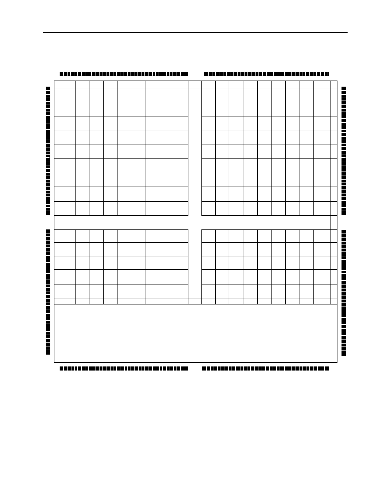
PT1 PT2 PT3 PT4 PT5 PT6 PT7 PT8 PT9 TMID PT10 PT11 PT12 PT13 PT14 PT15 PT16 PT17 PT18
R1C1 R1C2 R1C3 R1C4 R1C5 R1C6 R1C7 R1C8 R1C9
R1C10 R1C11 R1C12 R1C13 R1C14 R1C15 R1C16 R1C17 R1C18
R2C1 R2C2 R2C3 R2C4 R2C5 R2C6 R2C7 R2C8 R2C9 vIQ R2C10 R2C11 R2C12 R2C13 R2C14 R2C15 R2C16 R2C17 R2C18
R3C1 R3C2 R3C3 R3C4 R3C5 R3C6 R3C7 R3C8 R3C9
R3C10 R3C11 R3C12 R3C13 R3C14 R3C15 R13C16 R3C17 R3C18
R4C1 R4C2 R4C3 R4C4 R4C5 R4C6 R4C7 R4C8 R4C9
R4C10 R4C11 R4C12 R4C13 R4C14 R4C15 R4C16 R4C17 R4C18
R5C1 R5C2 R5C3 R5C4 R5C5 R5C6 R5C7 R5C8 R5C9
R5C10 R5C11 R5C12 R5C13 R5C14 R5C15 R5C16 R5C17 R5C18
R6C1 R6C2 R6C3 R6C4 R6C5 R6C6 R6C7 R6C8 R6C9
R6C10 R6C11 R6C12 R6C13 R6C14 R6C15 R6C16 R6C17 R6C18
R7C1 R7C2 R7C3 R7C4 R7C5 R7C6 R7C7 R7C8 R7C9
R7C10 R7C11 R7C12 R7C13 R7C14 R7C15 R7C16 R7C17 R7C18
R8C1 R8C2 R8C3 R8C4 R8C5 R8C6 R8C7 R8C8 R8C9
R8C10 R8C11 R8C12 R8C13 R8C14 R8C15 R8C16 R8C17 R8C18
R9C1 R9C2 R9C3 R9C4 R9C5 R9C6 R9C7 R9C8 R9C9
hIQ
R10C1 R10C2 R10C3 R10C4 R10C5 R10C6 R10C7 R10C8 R10C9
R9C10 R9C11 R9C12 R9C13 R9C14 R9C15 R9C16 R9C17 R9C18
R10C10 R10C11 R10C12 R10C13 R10C14 R10C15 R10C16 R10C17 R10C18
R11C1 R11C2 R11C3 R11C4 R11C5 R11C6 R11C7 R11C8 R11C9
R11C10 R11C11 R11C12 R11C13 R11C14 R11C15 R11C16 R11C17 R11C18
R12C1 R12C2 R12C3 R12C4 R12C5 R12C6 R12C7 R12C8 R12C9
R12C10 R12C11 R12C12 R12C13 R12C14 R12C15 R12C16 R12C17 R12C18
R13C1 R13C2 R13C3 R13C4 R13C5 R13C6 R13C7 R13C8 R13C9
R13C10 R13C11 R13C12 R13C13 R13C14 R13C15 R13C16 R13C17 R13C18
R14C1 R14C2 R14C3 R14C4 R14C5 R14C6 R14C7 R14C8 R14C9
R14C10 R14C11 R14C12 R14C13 R14C14 R14C15 R14C16 R14C17 R14C18
PB1 PB2 PB3 PB4 PB5 PB6 PB7 PB8 PB9 BMIDT PB10 PB11 PB12 PB13 PB14 PB15 PB16 PB17 PB18
EMBEDDED CORE AREA
Figure 1. OR3TP12 Array
5-4489(F).b
Lucent Technologies Inc.
Lucent Technologies Inc.
11
11 Page | ||
| Páginas | Total 30 Páginas | |
| PDF Descargar | [ Datasheet OR3TP12.PDF ] | |
Hoja de datos destacado
| Número de pieza | Descripción | Fabricantes |
| OR3TP12 | Field-Programmable System Chip (FPSC) Embedded Master/Target PCI Interface | Agere Systems |
| Número de pieza | Descripción | Fabricantes |
| SLA6805M | High Voltage 3 phase Motor Driver IC. |
Sanken |
| SDC1742 | 12- and 14-Bit Hybrid Synchro / Resolver-to-Digital Converters. |
Analog Devices |
|
DataSheet.es es una pagina web que funciona como un repositorio de manuales o hoja de datos de muchos de los productos más populares, |
| DataSheet.es | 2020 | Privacy Policy | Contacto | Buscar |
