|
|
|
PDF ST24FC21B Data sheet ( Hoja de datos )
| Número de pieza | ST24FC21B | |
| Descripción | 1 Kbit x8 Dual Mode Serial EEPROM for VESA PLUG & PLAY | |
| Fabricantes | ST Microelectronics | |
| Logotipo | ||
Hay una vista previa y un enlace de descarga de ST24FC21B (archivo pdf) en la parte inferior de esta página. Total 22 Páginas | ||
|
No Preview Available !
ST24LC21B, ST24LW21
ST24FC21, ST24FC21B, ST24FW21
1 Kbit (x8) Dual Mode Serial EEPROM
for VESA PLUG & PLAY
1 MILLION ERASE/WRITE CYCLES
40 YEARS DATA RETENTION
3.6V to 5.5V or 2.5V to 5.5V SINGLE SUPPLY
VOLTAGE
HARDWARE WRITE CONTROL (ST24LW21
and ST24FW21)
TTL SCHMITT-TRIGGER on VCLK INPUT
100k / 400k Hz COMPATIBILITY with the I2C
BUS BIT TRANSFER RANGE
TWO WIRE SERIAL INTERFACE I2C BUS
COMPATIBLE
I2C PAGE WRITE (up to 8 Bytes)
I2C BYTE, RANDOM and SEQUENTIAL READ
MODES
SELF TIMED PROGRAMMING CYCLE
AUTOMATIC ADDRESS INCREMENTING
ENHANCED ESD/LATCH UP
PERFORMANCES
ERROR RECOVERY MECHANISM
(ST24FC21 and ST24FW21) VESA 2
COMPATIBLE
DESCRIPTION
The ST24LC21B, ST24LW21, ST24FC21,
ST24FC21B and ST24FW21 are 1K bit electrically
erasable programmable memory (EEPROM), or-
ganized in 128x8 bits. In the text, products are
referred as ST24xy21, where "x" is either "L" for
VESA 1 or "F" for VESA 2 compatible memories
and where "y" indicates the Write Control pin con-
nection: "C" means WC on pin 7 and "W" means
WC on pin 3.
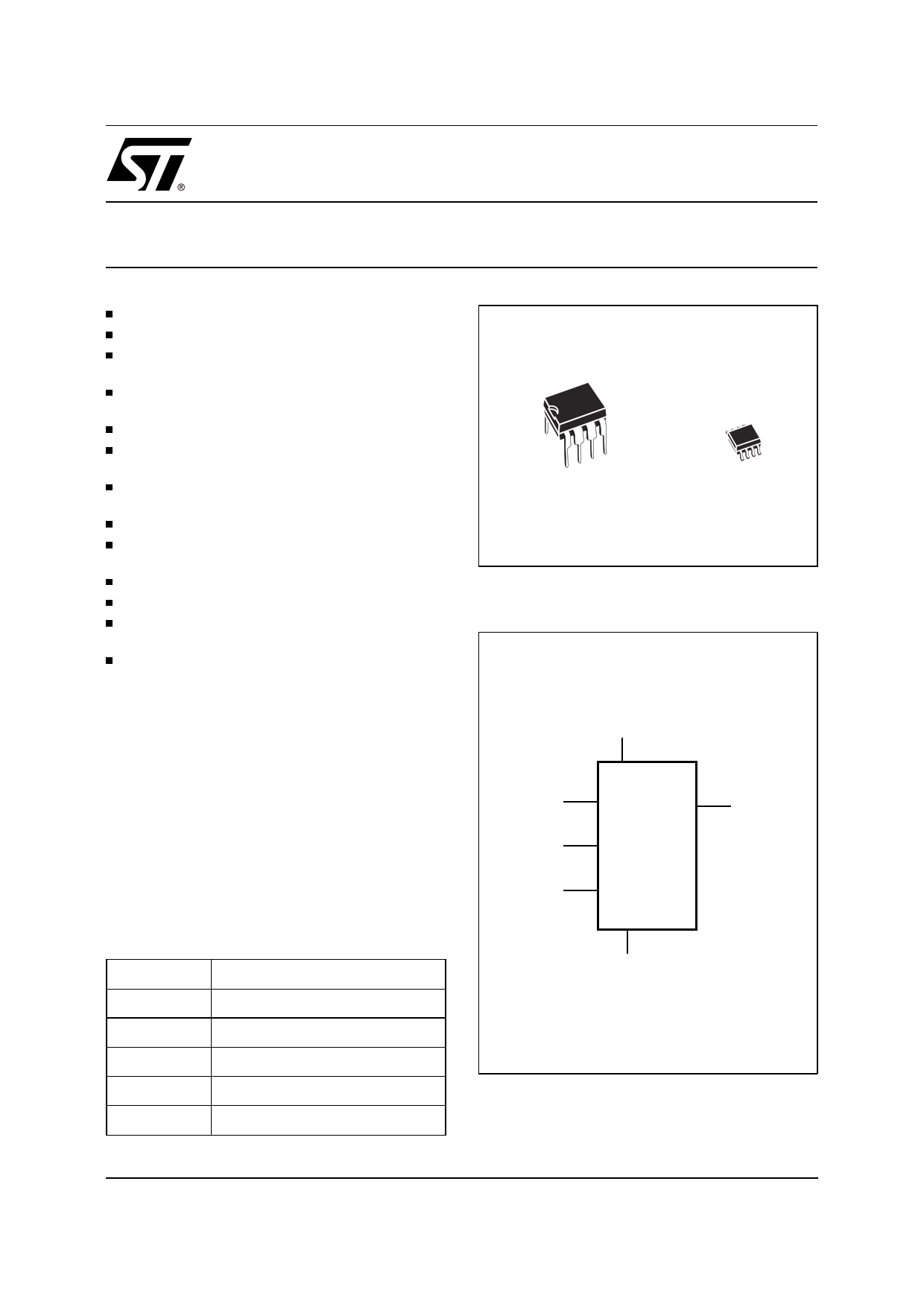
8
1
PSDIP8 (B)
0.25mm Frame
8
1
SO8 (M)
150mil Width
Figure 1. Logic Diagram
VCC
SCL
VCLK
WC
ST24xy21
SDA
Table 1. Signal Names
SDA
SCL
Serial Data Address Input/Output
Serial Clock (I2C mode)
VCC
VSS
VCLK
Supply Voltage
Ground
Clock Transmit only mode
WC Write Control
June 2002
VSS
AI01741
Note: WC signal is only available for ST24LW21 and ST24FW21
products.
1/22
1 page 
ST24LC21B, ST24LW21, ST24FC21, ST24FC21B, ST24FW21
Figure 4. Transition from Transmit Only (DDC1) to Bi-directional (DDC2B) Mode Waveforms
SCL
SDA
Transmit Only Mode
- Temporary Bi-Directional Mode
(ST24FC21 and ST24FW21)
- Locked Bi-Directional Mode
(ST24LC21B and ST24LW21)
12
MSB
- Locked Bi-Directional
Mode (ST24FC21
and ST24FW21)
89
ACK
VCLK
START
CONDITION
AI01892
A byte is clocked out (on SDA pin) with nine clock
pulses on VCLK: 8 clock pulses for the data byte
and one extra clock pulse for a Don’t Care bit.
As long as the SCL pin is held high, each byte of
the memory array is transmitted serially on the SDA
pin with an automatic address increment.
When the last byte is transmitted, the address
counter will roll-over to location 00h.
I2C Bidirectional Mode
The ST24xy21 can be switched from Transmit Only
mode to I2C Bidirectional mode by applying a valid
high to low transition on the SCL pin (see Figure 4).
– When the ST24LC21B (or the ST24FC21 or
the ST24FC21B) is in the I2C Bidirectional
mode, the VCLK input (pin 7) enables (or inhib-
its) the execution of any write instruction: if
VCLK = 1, write instructions are executed; if
VCLK = 0, write instructions are not executed.
– When the ST24LW21 (or the ST24FW21) is in
the I2C Bidirectional mode, the Write Control
(WC on pin 3) input enables (or inhibits) the
execution of any write instruction: if WC = 1,
write instructions are executed;if WC = 0,
write instructions are not executed.
The ST24xy21 is compatible with the I2C standard,
two wire serial interface which uses a bidirectional
data bus and serial clock. The ST24xy21 carries a
built-in 4 bit, unique device identification code
(1010) named Device Select code corresponding
to the I2C bus definition. The ST24LC21B carries a
unique device identification code (1010.0000 RW)
named Device Select code corresponding to the
I2C bus definition.
The ST24xy21 behaves as a slave device in the
I2C protocol with all memory operations synchro-
nized by the serial clock SCL. Read and write
operations are initiated by a START condition gen-
erated by the bus master. The START condition is
followed by a stream of 7 bits, plus one read/write
bit and terminated by an acknowledge bit.
When data is written into the memory, the
ST24xy21 responds to the 8 bits received by as-
serting an acknowledge bit during the 9th bit time.
When data is read by the bus master, it must
acknowledge the receipt of the data bytes in the
same way. Data transfers are terminated with a
STOP condition (see READ and WRITE descrip-
tions in the following pages).
Power On Reset: VCC lock out write protect
In order to prevent data corruption and inadvertent
write operations during power up, a Power On
Reset (POR) circuit is implemented. Until the VCC
voltage has reached the POR threshold value, the
internal reset is active, all operations are disabled
and the device will not respond to any command.
In the same way, when VCC drops down from the
operating voltage to below the POR threshold
value, all operations are disabled and the device
will not respond to any command. A stable VCC
must be applied before applying any logic signal.
Error Recovery Modes available in the
ST24FC21, ST24FC21B and the ST24FW21
5/22
5 Page 
ST24LC21B, ST24LW21, ST24FC21, ST24FC21B, ST24FW21
Table 8. AC Characteristics, I2C Bidirectional Mode for Clock Frequency = 100kHz
(TA = –40 to 85 °C; VCC = 3.6V to 5.5V)
Symbol
Alt
Parameter
Min Max Unit
tCH1CH2
tR Clock Rise Time
1 µs
tCL1CL2
tF Clock Fall Time
300 ns
tDH1DH2
tR Input Rise Time
1 µs
tDL1DL1
tCHDX (1)
tF
tSU:STA
Input Fall Time
Clock High to Input Transition
300 ns
4.7 µs
tCHCL
tHIGH
Clock Pulse Width High
4 µs
tDLCL
tHD:STA
Input Low to Clock Low (START)
4
µs
tCLDX
tHD:DAT
Clock Low to Input Transition
0 µs
tCLCH
tLOW
Clock Pulse Width Low
4.7 µs
tDXCX
tSU:DAT
Input Transition to Clock Transition
250
ns
tCHDH
tSU:STO
Clock High to Input High (STOP)
4.7
µs
tDHDL
tCLQV (2)
tBUF Input High to Input Low (Bus Free)
tAA Clock Low to Next Data Out Valid
4.7 µs
0.2 3.5 µs
tCLQX
tDH Data Out Hold Time
200 ns
fC fSCL Clock Frequency
100 kHz
tW tWR Write Time
10 ms
Notes: 1. For a reSTART condition, or following a write cycle.
2. The minimum value delays the falling/rising edge of SDA away from SCL = 1 in order to avoid unwanted START and/or STOP
conditions.
Table 9. AC Characteristics, Transmit-only Mode
(TA = –40 to 85 °C; VCC = 3.6V to 5.5V)
Symbol
Alt
Parameter
tVCHQX
tVAA Output Valid from VCLK
tVCHVCL
tVHIGH
VCLK High Time
tVCLVCH
tVLOW
VCLK Low Time
tCLQZ
tVHZ Mode Tansition Time
tVPU (1,2)
Transmit-only Power-up Time
tVH1VH2 (2)
tR VCLK Rise Time
tVL1VL2 (2)
tF VCLK Fall Time
tRECOVERY (2)
Recovery Time
Notes: 1. Refer to Figure 3.
2. Sampled only, not 100% tested.
Min Max Unit
500 ns
600 ns
1.3 µs
500 ns
0 ns
1 µs
1 µs
1.5 3.5 sec
11/22
11 Page | ||
| Páginas | Total 22 Páginas | |
| PDF Descargar | [ Datasheet ST24FC21B.PDF ] | |
Hoja de datos destacado
| Número de pieza | Descripción | Fabricantes |
| ST24FC21 | (ST24xx21B) 1 Kbit x8 Dual Mode Serial EEPROM | STMicroelectronics |
| ST24FC21B | 1 Kbit x8 Dual Mode Serial EEPROM for VESA PLUG & PLAY | ST Microelectronics |
| ST24FC21B | (ST24xx21B) 1 Kbit x8 Dual Mode Serial EEPROM | STMicroelectronics |
| Número de pieza | Descripción | Fabricantes |
| SLA6805M | High Voltage 3 phase Motor Driver IC. |
Sanken |
| SDC1742 | 12- and 14-Bit Hybrid Synchro / Resolver-to-Digital Converters. |
Analog Devices |
|
DataSheet.es es una pagina web que funciona como un repositorio de manuales o hoja de datos de muchos de los productos más populares, |
| DataSheet.es | 2020 | Privacy Policy | Contacto | Buscar |