|
|
|
PDF TC1227 Data sheet ( Hoja de datos )
| Número de pieza | TC1227 | |
| Descripción | (TC1225 / TC1226 / TC1227) Inverting Dual Charge Pump Voltage Converters | |
| Fabricantes | Microchip Technology | |
| Logotipo | ||
Hay una vista previa y un enlace de descarga de TC1227 (archivo pdf) en la parte inferior de esta página. Total 10 Páginas | ||
|
No Preview Available !
TC1225
TC1226
TC1227
Inverting Dual (–VIN, –2VIN) Charge Pump Voltage Converters
FEATURES
s Small 8-Pin MSOP Package
s Operates from 1.8V to 5.5V
s Up to 5mA Output Current at –VIN Pin
s Up to 1mA Output Current at –2VIN Pin
s –VIN and –2VIN Outputs Available
s Low Supply Current
.......................................... 120µA (MAX) for TC1225
.......................................... 360µA (MAX) for TC1226
.......................................... 1.5mA (MAX) for TC1227
TYPICAL APPLICATIONS
s LCD Panel Bias
s Cellular Phones PA Bias
s Pagers
s PDAs, Portable Data loggers
s Battery Powered Devices
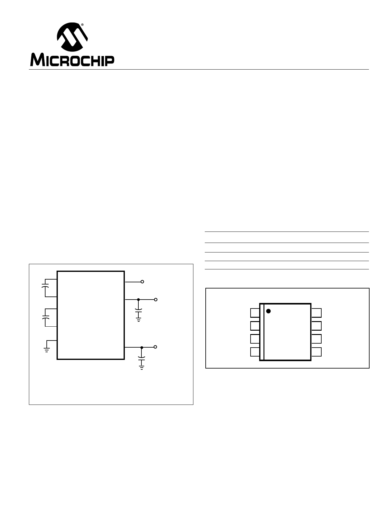
TYPICAL OPERATING CIRCUIT
+ C1+
C1
VIN INPUT
C1– –VIN OUTPUT 1
C2+ – COUT1
+ TC1225
+
C2 TC1226
C2– TC1227
GND
–2 VIN
OUTPUT 2
– COUT2
+
Notes:
1) C1 and COUT1 must have a voltage rating greater
than or equal to VIN
2) C2 and COUT2 must have a voltage rating greater
than or equal to 2VIN
GENERAL DESCRIPTION
The TC1225/1226/1227 are CMOS dual inverting charge
pump voltage converters in 8-Pin MSOP packages. An on-
board oscillator provides the clock, and only four external
capacitors are required for full circuit implementation. Switch-
ing frequencies are 12kHz for the TC1225, 35kHz for the
TC1226, and 125kHz for the TC1227.
These devices provide both a negative voltage inversion
(available at the –VIN output) and a negative doubling
voltage inversion (available at the –2 VIN output), with a low
output impedance capable of providing output currents up to
5mA for the –VIN output and 1mA for the –2VIN output. The
input voltage can range from +1.8V to +5.5V.
ORDERING INFORMATION
Part No. Package Osc Freq (kHz) Temp Range
TC1225EUA 8-Pin MSOP
TC1226EUA 8-Pin MSOP
TC1227EUA 8-Pin MSOP
12
35
125
–40°C to +85°C
–40°C to +85°C
–40°C to +85°C
PIN CONFIGURATION
8-Pin MSOP
C1– 1
C2+ 2
C2– 3
–2VIN 4
TC1225
TC1226
TC1227
8 –VIN
7 C1+
6 VIN
5 GND
© 2001 Microchip Technology Inc. DS21369A
TC1225/6/7-1 3/24/00
1 page 
Inverting Dual (–VIN, –2VIN)
Charge Pump Voltage Converters
TC1225
TC1226
TC1227
Dual Voltage Inverter
The most common application for the TC1225/1226/
1227 devices is the dual voltage inverter (Figure 2). This
application uses four external capacitors: C1, C2, COUT1,
and COUT2 (NOTE: a power supply bypass capacitor is
recommended). The outputs are equal to – VIN and –2VIN
plus any voltage drops due to loading. Refer to Tables 1a,
1b, 2a, and 2b for capacitor selection guidelines.
Device
TC1225
TC1226
TC1227
CIN C1
3.3µF 3.3µF
1µF 1µF
0.33µF 0.33µF
C2
1µF
0.33µF
0.1µF
COUT1
3.3µF
1µF
0.33µF
COUT2
1µF
0.33µF
0.1µF
VIN
CIN
C1
C2
7 C1+
1 C1–
2 C2+
3 C2–
6
VIN
–VIN 8
COUT1
TC1225
TC1226
TC1227
4
–2VIN
COUT2
GND
5
RL1
RL2
VOUT1
VOUT2
Figure 3 is a schematic of the TC1225 DEMO Card, and
Figure 4 shows the assembly drawing and artwork for the
board. Table 3 lists the voltages that are monitored by the
test points and Table 4 lists the currents that can be
measured using the jumpers.
Table 3. TC1225 DEMO Card Test Points
TEST POINT VOLTAGE MEASUREMENT
TP1 VIN [+5V]
TP2 GROUND
TP3 GROUND
TP4 TCM828 U1 OUTPUT [-5V(1)]
TP5 TCM828 U2 OUTPUT [-10V(1)]
TP6 TC1225 STAGE 1 OUTPUT [-5V(2)]
TP7 TC1225 STAGE 2 OUTPUT [-10V(2)]
Table 4. TC1225 DEMO Card Jumpers
JUMPER
CURRENT MEASUREMNT
J1 DUAL TCM828 QUIESCENT CURRENT
J2 TC1225 QUIESCENT CURRENT
J3 TCM828 U1 [-5V(1)] LOAD CURRENT
J4 TCM828 U2 [-10V(1)] LOAD CURRENT
J5 TC1225 STAGE 1 [-5V(2)] LOAD CURRENT
J6 TC1225 STAGE 2 [-10V(2)] LOAD CURRENT
Figure 2. Dual Voltage Inverter Test Circuit
Layout Considerations
As with any switching power supply circuit good layout
practice is recommended. Mount components as close
together as possible to minimize stray inductance and
capacitance. Also use a large ground plane to minimize
noise leakage into other circuitry.
TC1225 DEMO CARD
The TC1225 DEMO Card is a 2.0” x 2.0” card containing
both a TC1225 and two cascaded TCM828s that allow the
user to compare the operation of each approach for gener-
ating a –1X and –2X function. Each circuit is fully assembled
with the required external capacitors along with variable
load resistors that allow the user to vary the output load
current of each stage. For convenience, several test points
and jumpers are available for measuring various voltages
and currents on the demo board.
© 2001 Microchip Technology Inc. DS21369A
5
TC1225/6/7-1 3/24/00
5 Page | ||
| Páginas | Total 10 Páginas | |
| PDF Descargar | [ Datasheet TC1227.PDF ] | |
Hoja de datos destacado
| Número de pieza | Descripción | Fabricantes |
| TC122 | TIRISTORI | M&G Electronic |
| TC122 | ARRAY CHIP RESISTORS | Yageo |
| TC122-20 | thyristors (triacs) | ETC |
| TC122-20 | thyristors (triacs) | ETC |
| Número de pieza | Descripción | Fabricantes |
| SLA6805M | High Voltage 3 phase Motor Driver IC. |
Sanken |
| SDC1742 | 12- and 14-Bit Hybrid Synchro / Resolver-to-Digital Converters. |
Analog Devices |
|
DataSheet.es es una pagina web que funciona como un repositorio de manuales o hoja de datos de muchos de los productos más populares, |
| DataSheet.es | 2020 | Privacy Policy | Contacto | Buscar |