|
|
PDF MC34161 Data sheet ( Hoja de datos )
| Número de pieza | MC34161 | |
| Descripción | Universal Voltage Monitors | |
| Fabricantes | ON Semiconductor | |
| Logotipo | ||
Hay una vista previa y un enlace de descarga de MC34161 (archivo pdf) en la parte inferior de esta página. Total 16 Páginas | ||
|
No Preview Available !
MC34161, MC33161
Universal Voltage Monitors
The MC34161/MC33161 are universal voltage monitors intended
for use in a wide variety of voltage sensing applications. These devices
offer the circuit designer an economical solution for positive and
negative voltage detection. The circuit consists of two comparator
channels each with hysteresis, a unique Mode Select Input for channel
programming, a pinned out 2.54 V reference, and two open collector
outputs capable of sinking in excess of 10 mA. Each comparator
channel can be configured as either inverting or noninverting by the
Mode Select Input. This allows over, under, and window detection of
positive and negative voltages. The minimum supply voltage needed
for these devices to be fully functional is 2.0 V for positive voltage
sensing and 4.0 V for negative voltage sensing.
Applications include direct monitoring of positive and negative
voltages used in appliance, automotive, consumer, and industrial
equipment.
• Unique Mode Select Input Allows Channel Programming
• Over, Under, and Window Voltage Detection
• Positive and Negative Voltage Detection
• Fully Functional at 2.0 V for Positive Voltage Sensing and 4.0 V for
Negative Voltage Sensing
• Pinned Out 2.54 V Reference with Current Limit Protection
• Low Standby Current
• Open Collector Outputs for Enhanced Device Flexibility
Simplified Block Diagram
(Positive Voltage Window Detector Application)
VCC
8
1
2.54V
Reference
VS 7
–
2
+
++
2.8V
+–
1.27V
–
3
+
++
0.6V
+–
1.27V
6
5
4
http://onsemi.com
8
1
8
1
PDIP–8
P SUFFIX
CASE 626
SO–8
D SUFFIX
CASE 751
MARKING
DIAGRAMS
8
MC3x161P
AWL
YYWW
1
8
3x161
ALYW
1
x = 3 or 4
A = Assembly Location
WL, L = Wafer Lot
YY, Y = Year
WW, W = Work Week
PIN CONNECTIONS
Vref 1
Input 1 2
Input 2 3
Gnd 4
8 VCC
7 Mode Select
6 Output 1
5 Output 2
(TOP VIEW)
ORDERING INFORMATION
Device
Package
Shipping
MC34161D
SO–8
98 Units/Rail
MC34161DR2
SO–8
2500 Tape & Reel
MC34161P
PDIP–8
50 Units/Rail
MC33161D
SO–8
98 Units/Rail
MC33161DR2
SO–8
2500 Tape & Reel
MC33161P
PDIP–8
50 Units/Rail
© Semiconductor Components Industries, LLC, 2000
April, 2000 – Rev. 2
1
Publication Order Number:
MC34161/D
1 page 
MC34161, MC33161
Vref
1
Mode Select
7
Input 1
+
2+ –
1.27V
Input 2
+
3+ –
1.27V
VCC
8
2.54V
Reference
–
++
2.8V
Channel 1
Output 1
6
–
++
0.6V
Channel 2
Output 2
5
Gnd 4
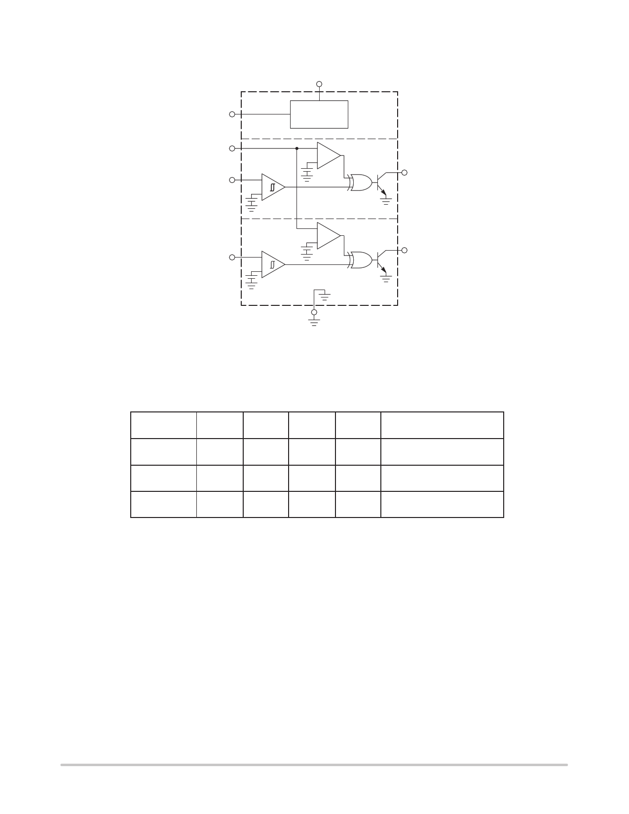
Figure 13. MC34161 Representative Block Diagram
Mode Select
Pin 7
GND
Vref
VCC (>2.0 V)
Input 1
Pin 2
0
1
0
1
0
1
Output 1
Pin 6
0
1
0
1
1
0
Input 2
Pin 3
0
1
0
1
0
1
Output 2
Pin 5
0
1
1
0
1
0
Comments
Channels 1 & 2: Noninverting
Channel 1: Noninverting
Channel 2: Inverting
Channels 1 & 2: Inverting
Figure 14. Truth Table
http://onsemi.com
5
5 Page 
MC34161, MC33161
Input VS
V2
V1
Output
Voltage
Pins 5, 6
Gnd
VCC
Gnd
VHys
Osc ‘ON’
VS
R2
R1
VCC
8
2.54V
1 Reference
7
+
2+ –
1.27V
+
3+ –
1.27V
–
++
2.8V
–
++
0.6V
4
RA
Piezo
6
5
CT RB
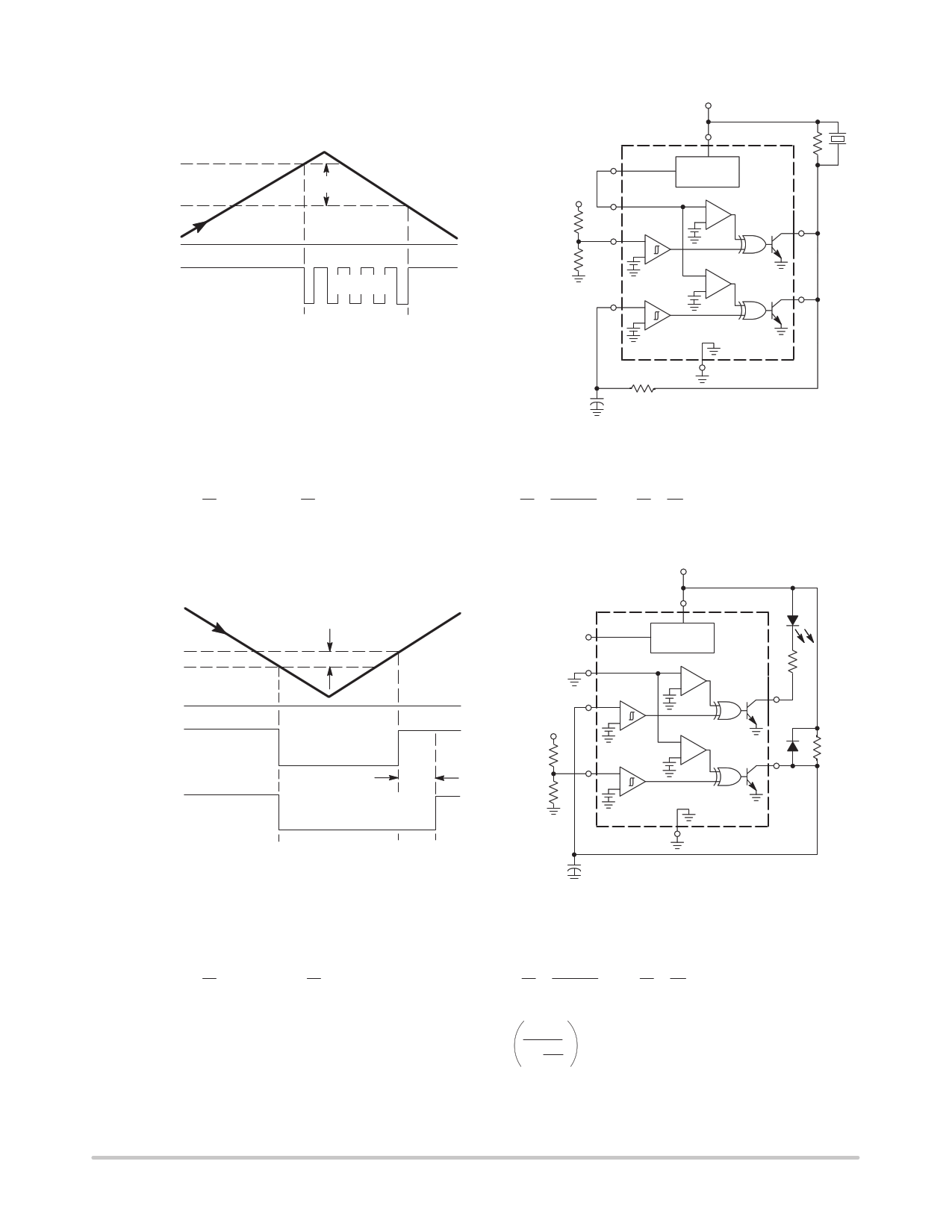
The above figure shows the MC34161 configured as an overvoltage detector with an audio alarm. Channel 1 monitors input voltage VS while channel 2 is connected
as a simple RC oscillator. As the input voltage increases from ground, the output of channel 1 allows the oscillator to turn ‘ON’ when VS exceeds V2.
For known resistor values, the voltage trip points are:
+ * ǒ ) Ǔ + ǒ ) ǓV1
(Vth
VH)
R2
R1
1 V2
Vth
R2
R1
1
For a specific trip voltage, the required resistor ratio is:
+ * * + *R2
R1
V1
Vth VH
1
R2
R1
V2
Vth
1
Figure 23. Overvoltage Detector with Audio Alarm
Input VS
V2
V1
Output
Voltage
Pin 5
Gnd
VCC
Gnd
Output
Voltage
Pin 6
VCC
Gnd
VHys
tDLY
Reset LED ‘ON’
VS
R2
R1
VCC
8
2.54V
1 Reference
7
+
2+ –
1.27V
+
3+ –
1.27V
–
++
2.8V
–
++
0.6V
4
R3
6
RDLY
5
CDLY
The above figure shows the MC34161 configured as a microprocessor reset with a time delay. Channel 2 monitors input voltage VS while channel 1 performs the
time delay function. As the input voltage decreases towards ground, the output of channel 2 quickly discharges CDLY when VS falls below V1. As the input voltage
increases from ground, the output of channel 2 allows RDLY to charge CDLY when VS exceeds V2.
For known resistor values, the voltage trip points are:
+ * ǒ ) Ǔ + ǒ ) ǓV1
(Vth
VH)
R2
R1
1
V2
Vth
R2
R1
1
For a specific trip voltage, the required resistor ratio is:
+ * * + *R2
R1
V1
Vth VH
1
R2
R1
V2
Vth
1
For known RDLY CDLY values, the reset time delay is:
tDLY = RDLYCDLY In
1
1
–
Vth
VCC
Figure 24. Microprocessor Reset with Time Delay
http://onsemi.com
11
11 Page | ||
| Páginas | Total 16 Páginas | |
| PDF Descargar | [ Datasheet MC34161.PDF ] | |
Hoja de datos destacado
| Número de pieza | Descripción | Fabricantes |
| MC34160 | MICROPROCESSOR VOLTAGE REGULATOR/ SUPERVISORY CIRCUIT | Motorola Semiconductors |
| MC34160 | (MC33160 / MC34160) Voltage Regulator and Supervisory Circuit | ON Semiconductor |
| MC34161 | UNIVERSAL VOLTAGE MONITORS | Motorola Semiconductors |
| MC34161 | Universal Voltage Monitors | ON Semiconductor |
| Número de pieza | Descripción | Fabricantes |
| SLA6805M | High Voltage 3 phase Motor Driver IC. |
Sanken |
| SDC1742 | 12- and 14-Bit Hybrid Synchro / Resolver-to-Digital Converters. |
Analog Devices |
|
DataSheet.es es una pagina web que funciona como un repositorio de manuales o hoja de datos de muchos de los productos más populares, |
| DataSheet.es | 2020 | Privacy Policy | Contacto | Buscar |
