|
|
|
PDF MTB60N06HD Data sheet ( Hoja de datos )
| Número de pieza | MTB60N06HD | |
| Descripción | TMOS POWER FET 60 AMPERES 60 VOLTS | |
| Fabricantes | Motorola Semiconductors | |
| Logotipo | ||
Hay una vista previa y un enlace de descarga de MTB60N06HD (archivo pdf) en la parte inferior de esta página. Total 12 Páginas | ||
|
No Preview Available !
MOTOROLA
SEMICONDUCTOR TECHNICAL DATA
Order this document
by MTB60N06HD/D
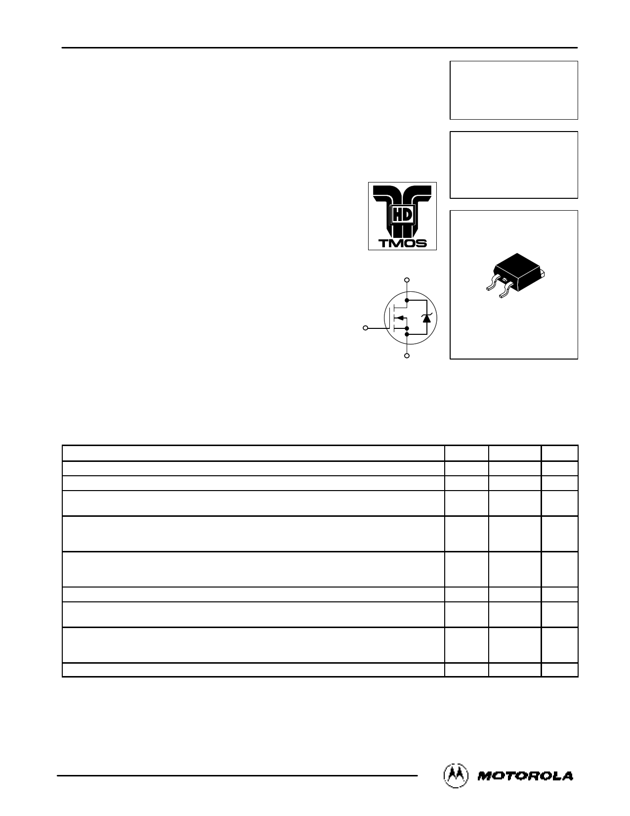
™Designer's Data Sheet
HDTMOS E-FET.™
High Energy Power FET
D2PAK for Surface Mount
N–Channel Enhancement–Mode Silicon Gate
The D2PAK package has the capability of housing a larger die
than any existing surface mount package which allows it to be used
in applications that require the use of surface mount components
with higher power and lower RDS(on) capabilities. This advanced
high–cell density HDTMOS power FET is designed to withstand
high energy in the avalanche and commutation modes. This new
energy efficient design also offers a drain–to–source diode with a
fast recovery time. Designed for low voltage, high speed switching
applications in power supplies, converters and PWM motor
controls, these devices are particularly well suited for bridge circuits
where diode speed and commutating safe operating areas are
critical and offer additional safety margin against unexpected
voltage transients.
• Avalanche Energy Specified
• Source–to–Drain Diode Recovery Time Comparable to a
Discrete Fast Recovery Diode
• Diode is Characterized for Use in Bridge Circuits
• IDSS and VDS(on) Specified at Elevated Temperature
• Short Heatsink Tab Manufactured — Not Sheared
• Specially Designed Leadframe for Maximum Power Dissipation
• Available in 24 mm 13–inch/800 Unit Tape & Reel, Add T4
Suffix to Part Number
G
MTB60N06HD
Motorola Preferred Device
TMOS POWER FET
60 AMPERES
60 VOLTS
RDS(on) = 0.014 OHM
™
D
CASE 418B–02, Style 2
D2PAK
S
MAXIMUM RATINGS (TC = 25°C unless otherwise noted)
Rating
Symbol
Value
Unit
Drain–Source Voltage
Drain–Gate Voltage (RGS = 1.0 MΩ)
Gate–Source Voltage — Continuous
Gate–Source Voltage — Non–Repetitive (tp ≤ 10 ms)
Drain Current — Continuous
Drain Current — Continuous @ 100°C
Drain Current — Single Pulse (tp ≤ 10 µs)
Total Power Dissipation
Derate above 25°C
Total Power Dissipation @ TA = 25°C (1)
Operating and Storage Temperature Range
Single Pulse Drain–to–Source Avalanche Energy — Starting TJ = 25°C
(VDD = 25 Vdc, VGS = 10 Vdc, Peak IL = 60 Apk, L = 0.3 mH, RG = 25 Ω)
Thermal Resistance — Junction to Case
Thermal Resistance — Junction to Ambient
Thermal Resistance — Junction to Ambient, when mounted with the minimum recommended pad size
Maximum Lead Temperature for Soldering Purposes, 1/8″ from case for 10 seconds
(1) When mounted with the minimum recommended pad size.
VDSS
VDGR
VGS
VGSM
ID
ID
IDM
PD
TJ, Tstg
EAS
RθJC
RθJA
RθJA
TL
60
60
± 20
± 30
60
42.3
180
125
1.0
2.5
– 55 to 150
540
1.0
62.5
50
260
Vdc
Vdc
Vdc
Vpk
Adc
Apk
Watts
W/°C
Watts
°C
mJ
°C/W
°C
Designer’s Data for “Worst Case” Conditions — The Designer’s Data Sheet permits the design of most circuits entirely from the information presented. SOA Limit
curves — representing boundaries on device characteristics — are given to facilitate “worst case” design.
E–FET, Designer’s and HDTMOS are trademarks of Motorola, Inc. TMOS is a registered trademark of Motorola, Inc.
Thermal Clad is a trademark of the Bergquist Company.
Preferred devices are Motorola recommended choices for future use and best overall value.
REV 2
© MMoototroorlao,lIancT. 1M99O5S Power MOSFET Transistor Device Data
1
1 page 
12
10
8
Q1
6
60
QT
50
VGS
40
Q2
30
4
ID = 60 A
20
TJ = 25°C
2 10
Q3
VDS
00
0 8 16 24 32 40 48 56
QT, TOTAL GATE CHARGE (nC)
Figure 8. Gate–To–Source and Drain–To–Source
Voltage versus Total Charge
1000
VDD = 30 V
ID = 60 A
VGS = 10 V
TJ = 25°C
100
tr
tf
td(off)
MTB60N06HD
td(on)
101 10
100
RG, GATE RESISTANCE (Ohms)
Figure 9. Resistive Switching Time
Variation versus Gate Resistance
DRAIN–TO–SOURCE DIODE CHARACTERISTICS
The switching characteristics of a MOSFET body diode
are very important in systems using it as a freewheeling or
commutating diode. Of particular interest are the reverse re-
covery characteristics which play a major role in determining
switching losses, radiated noise, EMI and RFI.
System switching losses are largely due to the nature of
the body diode itself. The body diode is a minority carrier de-
vice, therefore it has a finite reverse recovery time, trr, due to
the storage of minority carrier charge, QRR, as shown in the
typical reverse recovery wave form of Figure 12. It is this
stored charge that, when cleared from the diode, passes
through a potential and defines an energy loss. Obviously,
repeatedly forcing the diode through reverse recovery further
increases switching losses. Therefore, one would like a
diode with short trr and low QRR specifications to minimize
these losses.
The abruptness of diode reverse recovery effects the
amount of radiated noise, voltage spikes, and current ring-
ing. The mechanisms at work are finite irremovable circuit
parasitic inductances and capacitances acted upon by high
di/dts. The diode’s negative di/dt during ta is directly con-
trolled by the device clearing the stored charge. However,
the positive di/dt during tb is an uncontrollable diode charac-
teristic and is usually the culprit that induces current ringing.
Therefore, when comparing diodes, the ratio of tb/ta serves
as a good indicator of recovery abruptness and thus gives a
comparative estimate of probable noise generated. A ratio of
1 is considered ideal and values less than 0.5 are considered
snappy.
Compared to Motorola standard cell density low voltage
MOSFETs, high cell density MOSFET diodes are faster
(shorter trr), have less stored charge and a softer reverse re-
covery characteristic. The softness advantage of the high
cell density diode means they can be forced through reverse
recovery at a higher di/dt than a standard cell MOSFET
diode without increasing the current ringing or the noise gen-
erated. In addition, power dissipation incurred from switching
the diode will be less due to the shorter recovery time and
lower switching losses.
60
VGS = 0 V
50 TJ = 25°C
40
30
20
10
0
0.5 0.6 0.7 0.8 0.9
VSD, SOURCE–TO–DRAIN VOLTAGE (VOLTS)
1.0
Figure 10. Diode Forward Voltage versus Current
Motorola TMOS Power MOSFET Transistor Device Data
5
5 Page 
PACKAGE DIMENSIONS
C
E
BV
4
123
S
A
–T–
SEATING
PLANE
G
K
J
D 3 PL
0.13 (0.005) M T
H
STYLE 2:
PIN 1. GATE
2. DRAIN
3. SOURCE
4. DRAIN
CASE 418B–02
ISSUE B
MTB60N06HD
NOTES:
1. DIMENSIONING AND TOLERANCING PER ANSI
Y14.5M, 1982.
2. CONTROLLING DIMENSION: INCH.
INCHES
DIM MIN MAX
A 0.340 0.380
B 0.380 0.405
C 0.160 0.190
D 0.020 0.035
E 0.045 0.055
G 0.100 BSC
H 0.080 0.110
J 0.018 0.025
K 0.090 0.110
S 0.575 0.625
V 0.045 0.055
MILLIMETERS
MIN MAX
8.64 9.65
9.65 10.29
4.06 4.83
0.51 0.89
1.14 1.40
2.54 BSC
2.03 2.79
0.46 0.64
2.29 2.79
14.60 15.88
1.14 1.40
Motorola TMOS Power MOSFET Transistor Device Data
11
11 Page | ||
| Páginas | Total 12 Páginas | |
| PDF Descargar | [ Datasheet MTB60N06HD.PDF ] | |
Hoja de datos destacado
| Número de pieza | Descripción | Fabricantes |
| MTB60N06HD | TMOS POWER FET 60 AMPERES 60 VOLTS | Motorola Semiconductors |
| MTB60N06HD | Power MOSFET ( Transistor ) | ON Semiconductor |
| Número de pieza | Descripción | Fabricantes |
| SLA6805M | High Voltage 3 phase Motor Driver IC. |
Sanken |
| SDC1742 | 12- and 14-Bit Hybrid Synchro / Resolver-to-Digital Converters. |
Analog Devices |
|
DataSheet.es es una pagina web que funciona como un repositorio de manuales o hoja de datos de muchos de los productos más populares, |
| DataSheet.es | 2020 | Privacy Policy | Contacto | Buscar |