|
|
|
PDF MC33972 Data sheet ( Hoja de datos )
| Número de pieza | MC33972 | |
| Descripción | Multiple Switch Detection Interface with Suppressed Wake-Up | |
| Fabricantes | Motorola Semiconductors | |
| Logotipo | ||
Hay una vista previa y un enlace de descarga de MC33972 (archivo pdf) en la parte inferior de esta página. Total 28 Páginas | ||
|
No Preview Available !
Freescale Semiconductor, Inc.
MOTOROLA
SEMICONDUCTOR TECHNICAL DATA
Document order number: MC33972
Rev 3.0, 12/2004
Advance Information
Multiple Switch Detection Interface
with Suppressed Wake-Up
The 33972 Multiple Switch Detection Interface with Suppressed Wake-Up is
designed to detect the closing and opening of up to 22 switch contacts. The
switch status, either open or closed, is transferred to the microprocessor unit
(MCU) through a serial peripheral interface (SPI). The device also features a
22-to-1 analog multiplexer for reading inputs as analog. The analog input
signal is buffered and provided on the AMUX output terminal for the MCU to
read.
The 33972 device has two modes of operation, Normal and Sleep. Normal
mode allows programming of the device and supplies switch contacts with
pullup or pulldown current as it monitors switch change of state. The Sleep
mode provides low quiescent current, which makes the 33972 ideal for
automotive and industrial products requiring low sleep state currents.
Features
• Designed to Operate 5.5 V ≤ VPWR ≤ 26 V
• Switch Input Voltage Range -14 V to VPWR, 40 V Max
• Interfaces Directly to Microprocessor Using 3.3 V/5.0 V SPI Protocol
• Selectable Wake-Up on Change of State
• Selectable Wetting Current (16 mA or 2.0 mA)
• 8 Programmable Inputs (Switches to Battery or Ground)
• 14 Switch-to-Ground Inputs
• VPWR Standby Current 100 µA Typical, VDD Standby Current 20 µA
Typical
• Active Interrupt (INT) on Change-of-Switch State
• Pb-Free Packaging Designated by Suffix Code EW
33972
MULTIPLE SWITCH
DETECTION INTERFACE WITH
SUPPRESSED WAKE-UP
DWB SUFFIX
EW (Pb-FREE) SUFFIX
CASE 1324-02
32-TERMINAL SOICW
ORDERING INFORMATION
Device
Temperature
Range (TA)
Package
MC33972DWB/R2
MC33972EW/R2
-40°C to 125°C
32 SOICW
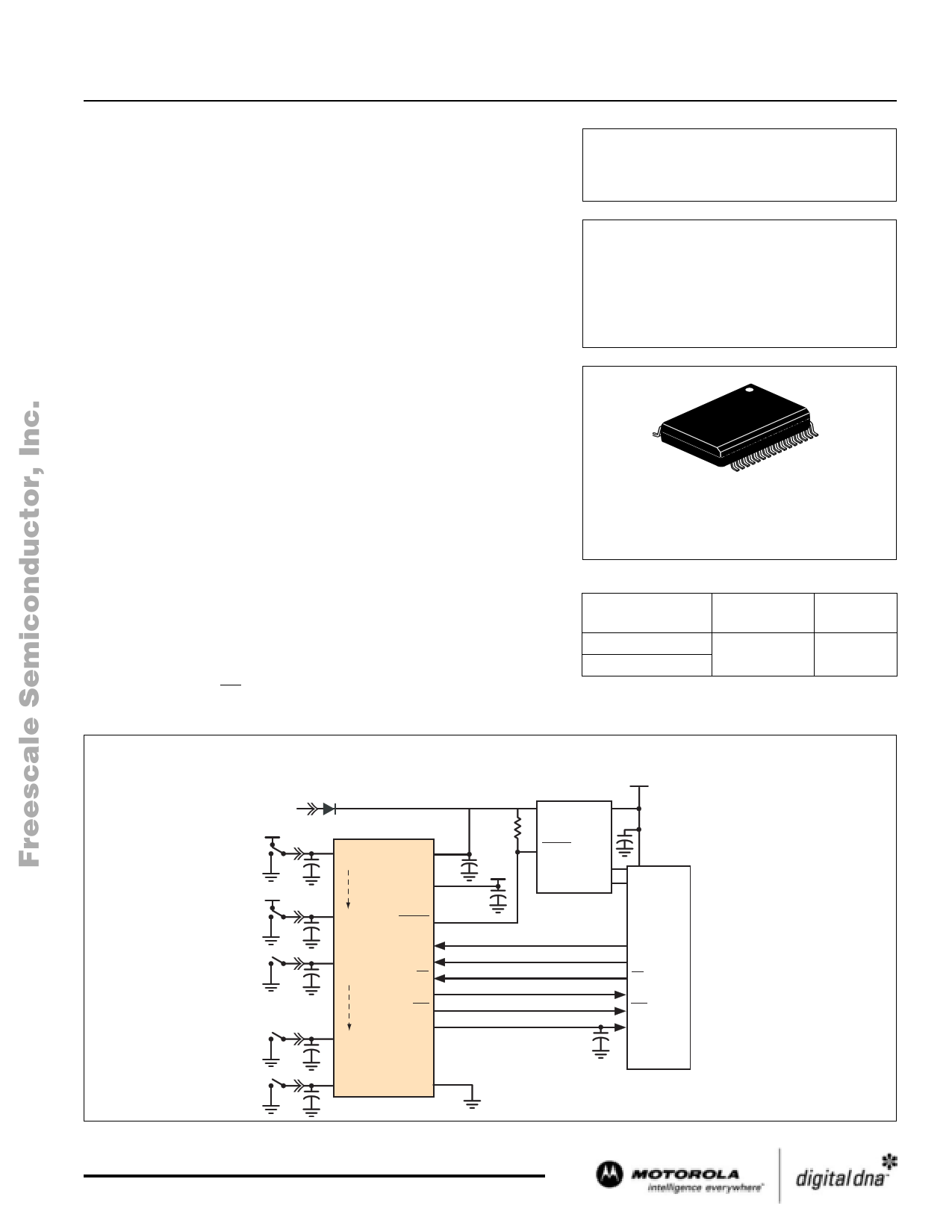
VBAT
VBAT
VBAT
3397S2imSpilmifiepdliAfipepdlicAaptiponlicDaiatigoranmDiagram
VDD
33972
SP0
SP1
VPWR
VDD
SP7
SG0
SG1
SG12
WAKE
SI
SCLK
CS
SO
INT
AMUX
Power Supply
LVI
Enable
Watchdog
Reset
MCU
MOSI
SCLK
CS
MISO
INT
AN0
SG13
GND
This document contains information on a new product.
Specifications and information herein are subject to change without notice.
© Motorola, Inc. 2004
For More Information On This Product,
Go to: www.freescale.com
1 page 
Freescale Semiconductor, Inc.
STATIC ELECTRICAL CHARACTERISTICS
Characteristics noted under conditions of 3.1 V ≤ VDD ≤ 5.25 V, 8.0 V ≤ VPWR ≤ 16 V, -40°C ≤ TC ≤ 125°C, unless otherwise noted.
Where applicable, typical values reflect the parameter’s approximate average value with VPWR = 13 V, TA = 25°C.
Characteristic
Symbol Min Typ Max Unit
POWER INPUT
Supply Voltage
Supply Voltage Range Quasi-Functional (Note 8)
Fully Operational
Supply Voltage Range Quasi-Functional (Note 8)
V
VPWR (QF)
5.5
–
8.0
VPWR (FO)
8.0
–
26
VPWR (QF)
26
–
40
Supply Current
All Switches Open, Normal Mode, Tri-State Disabled
IPWR (ON)
–
mA
2.0 4.0
Sleep State Supply Current
Scan Timer = 64 ms, Switches Open
IPWR (SS)
40
µA
70 100
Logic Supply Voltage
Logic Supply Current
All Switches Open, Normal Mode
Sleep State Logic Supply Current
Scan Timer = 64 ms, Switches Open
VDD 3.1 – 5.25 V
IDD mA
– 0.25 0.5
IDD(SS)
–
µA
10 20
SWITCH INPUT
Pulse Wetting Current Switch-to-Battery (Current Sink)
IPULSE
12
15
18 mA
Pulse Wetting Current Switch-to-Ground (Current Source)
IPULSE
12
16
18 mA
Sustain Current Switch-to-Battery Input (Current Sink)
ISUSTAIN
1.8
2.0
2.2 mA
Sustain Current Switch-to-Ground Input (Current Source)
ISUSTAIN
1.8
2.0
2.2 mA
Sustain Current Matching Between Channels on Switch-to-Ground Inputs
IMATCH
%
ISUS(MAX) - ISUS(MIN)
ISUS(MIN)
X 100
– 2.0 4.0
Input Offset Current When Selected as Analog
Input Offset Voltage When Selected as Analog
V(SP&SGinputs) to AMUX Output
IOFFSET
VOFFSET
-2.0
-10
1.4
2.5
2.0 µA
mV
10
Analog Operational Amplifier Output Voltage
Sink 250 µA
VOL mV
– 10 30
Analog Operational Amplifier Output Voltage
Source 250 µA
VOH
VDD - 0.1
–
V
–
Switch Detection Threshold
VTH
3.70 4.0
4.3 V
Switch Input Voltage Range
Temperature Monitor (Note 9), (Note 10)
Temperature Monitor Hysteresis (Note 10)
VIN -14 – 40 V
TLIM 155 – 185 °C
TLIM(HYS)
5.0
10
15 °C
Notes
8. Device operational. Table parameters may be out of specification.
9. Thermal shutdown of 16 mA pullup and pulldown current sources only. 2.0 mA current source/sink and all other functions remain active.
10. This parameter is guaranteed by design but is not production tested.
MOTOROLA ANALOG INTEGRATED CIRCUIT DEVICE DATA
For More Information On This Product,
Go to: www.freescale.com
33972
5
5 Page 
Freescale Semiconductor, Inc.
MCU INTERFACE DESCRIPTION
The 33972 device directly interfaces to a 3.3 V or 5.0 V
microcontroller unit (MCU). SPI serial clock frequencies up to
6.0 MHz may be used for programming and reading switch
input status (production tested at 4.16 MHz). Figure 5 illustrates
the configuration between an MCU and one 33972.
Serial peripheral interface (SPI) data is sent to the 33972
device through the SI input terminal. As data is being clocked
into the SI terminal, status information is being clocked out of
the device by the SO output terminal. The response to a SPI
command will always return the switch status, interrupt flag, and
thermal flag. Input switch states are latched into the SO register
on the falling edge of the chip select (CS) terminal. Twenty-four
bits are required to complete a transfer of information between
the 33972 and the MCU.
MC68HCXX
Microcontroller
Shift Register
MOSI
MISO
33972
SI
24-Bit Shift Register
SO
MC68HCXX
Microcontroller
Shift Register
MOSI
MISO
SCLK
Parallel
Ports
INT
33972
SI
SO
SCLK
CS
INT
33972
SI
SO
SCLK
CS
INT
SCLK
Figure 6. SPI Parallel Interface with Microprocessor
Receive
Buffer
Parallel
Ports
INT
To Logic
CS
INT
Figure 5. SPI Interface with Microprocessor
Two or more 33972 devices may be used in a module
system. Multiple ICs may be SPI-configured in parallel or serial.
Figures 6 and 7 show the configurations. When using the serial
configuration, 48-clock cycles are required to transfer data in/
out of the ICs.
MC68HCXX
Microcontroller
Shift Register
MOSI
MISO
SCLK
Parallel
Ports
INT
33972
SI
SO
SCLK
CS
INT
33972
SI
SO
SCLK
CS
INT
Figure 7. SPI Serial Interface with Microprocessor
MOTOROLA ANALOG INTEGRATED CIRCUIT DEVICE DATA
For More Information On This Product,
Go to: www.freescale.com
33972
11
11 Page | ||
| Páginas | Total 28 Páginas | |
| PDF Descargar | [ Datasheet MC33972.PDF ] | |
Hoja de datos destacado
| Número de pieza | Descripción | Fabricantes |
| MC33970 | Dual Gauge Driver Integrated Circuit | Freescale Semiconductor |
| MC33972 | Multiple Switch Detection Interface with Suppressed Wake-Up | Motorola Semiconductors |
| MC33972A | Multiple Switch Detection Interface | Freescale Semiconductor |
| MC33975 | Multiple Switch Detection Interface | Freescale Semiconductor |
| Número de pieza | Descripción | Fabricantes |
| SLA6805M | High Voltage 3 phase Motor Driver IC. |
Sanken |
| SDC1742 | 12- and 14-Bit Hybrid Synchro / Resolver-to-Digital Converters. |
Analog Devices |
|
DataSheet.es es una pagina web que funciona como un repositorio de manuales o hoja de datos de muchos de los productos más populares, |
| DataSheet.es | 2020 | Privacy Policy | Contacto | Buscar |