|
|
|
PDF ADCMP562 Data sheet ( Hoja de datos )
| Número de pieza | ADCMP562 | |
| Descripción | (ADCMP561 / ADCMP562) Dual High Speed PECL Comparators | |
| Fabricantes | Analog Devices | |
| Logotipo | ||
Hay una vista previa y un enlace de descarga de ADCMP562 (archivo pdf) en la parte inferior de esta página. Total 16 Páginas | ||
|
No Preview Available !
Dual High Speed PECL Comparators
ADCMP561/ADCMP562
FEATURES
Differential PECL compatible outputs
700 ps propagation delay input to output
75 ps propagation delay dispersion
Input common-mode range: –2.0 V to +3.0 V
Robust input protection
Differential latch control
Internal latch pull-up resistors
Power supply rejection greater than 85 dB
700 ps minimum pulse width
1.5 GHz equivalent input rise time bandwidth
Typical output rise/fall time of 500 ps
ESD protection > 4kV HBM, >200V MM
Programmable hysteresis
APPLICATIONS
Automatic test equipment
High speed instrumentation
Scope and logic analyzer front ends
Window comparators
High speed line receivers
Threshold detection
Peak detection
High speed triggers
Patient diagnostics
Disk drive read channel detection
Hand-held test instruments
Zero-crossing detectors
Line receivers and signal restoration
Clock drivers
GENERAL DESCRIPTION
The ADCMP561/ADCMP562 are high speed comparators
fabricated on Analog Devices’ proprietary XFCB process. The
devices feature a 700 ps propagation delay with less than 75 ps
overdrive dispersion. Dispersion, a measure of the difference in
propagation delay under differing overdrive conditions, is a
particularly important characteristic of comparators. A separate
programmable hysteresis pin is available on the ADCMP562.
A differential input stage permits consistent propagation delay
with a wide variety of signals in the common-mode range from
−2.0 V to +3.0 V. Outputs are complementary digital signals that
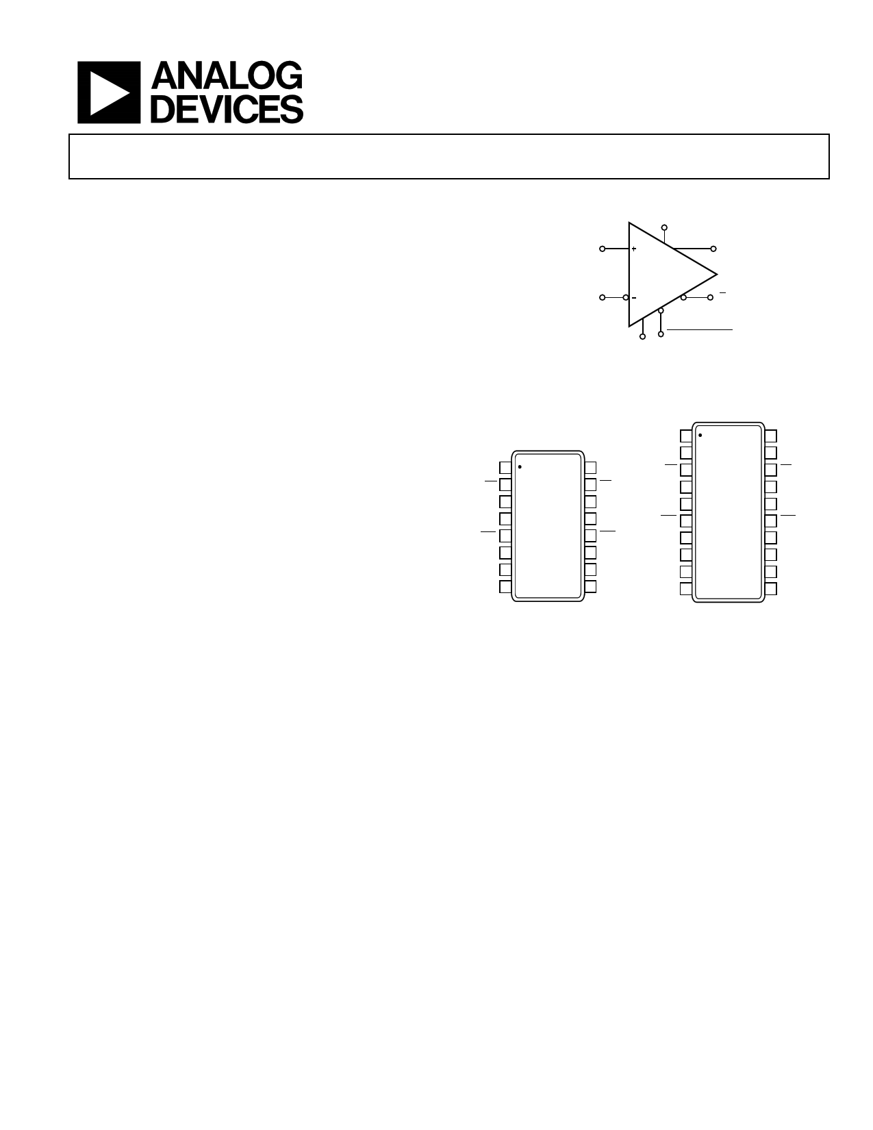
FUNCTIONAL BLOCK DIAGRAM
HYS*
NONINVERTING
INPUT
INVERTING
INPUT
ADCMP561/
ADCMP562
Q OUTPUT
Q OUTPUT
LATCH ENABLE
INPUT
LATCH ENABLE
INPUT
*ADCMP562 ONLY
Figure 1.
QA 1
16 QB
QA 2
15 QB
VDD 3
LEA 4
LEA 5
ADCMP561
TOP VIEW
(Not to Scale)
14 GND
13 LEB
12 LEB
VEE 6
–INA 7
11 VCC
10 –INB
+INA 8
9 +INB
VDD 1
20 VDD
QA 2
19 QB
QA 3
VDD 4
LEA 5
LEA 6
18 QB
ADCMP562 17 GND
TOP VIEW
(Not to Scale)
16 LEB
15 LEB
VEE 7
14 VCC
–INA 8
13 –INB
+INA 9
12 +INB
HYSA 10
11 HYSB
Figure 2. ADCMP561 16-Lead QSOP Figure 3. ADCMP562 20-Lead QSOP
are fully compatible with PECL 10 K and 10 KH logic families.
The outputs provide sufficient drive current to directly drive
transmission lines terminated in 50 Ω to VDD − 2 V. A latch
input, which is included, permits tracking, track-and-hold, or
sample-and-hold modes of operation. The latch input pins
contain internal pull-ups that set the latch in tracking mode
when left open.
The ADCMP561/ADCMP562 are specified over the industrial
temperature range (−40°C to +85°C).
Rev. A
Information furnished by Analog Devices is believed to be accurate and reliable.
However, no responsibility is assumed by Analog Devices for its use, nor for any
infringements of patents or other rights of third parties that may result from its use.
Specifications subject to change without notice. No license is granted by implication
or otherwise under any patent or patent rights of Analog Devices. Trademarks and
registered trademarks are the property of their respective owners.
One Technology Way, P.O. Box 9106, Norwood, MA 02062-9106, U.S.A.
Tel: 781.329.4700
www.analog.com
Fax: 781.326.8703 © 2004 Analog Devices, Inc. All rights reserved.
1 page 
ABSOLUTE MAXIMUM RATINGS
Table 2.
Parameter
Rating
Supply Voltages
Positive Supply Voltage (VCC to GND)
Negative Supply Voltage (VEE to GND)
Logic Supply Voltage (VDD to GND)
Ground Voltage Differential
−0.5 V to +6.0 V
−6.0 V to +0.5 V
−0.5 V to +6.0 V
−0.5 V to +0.5 V
Input Voltages
Input Common-Mode Voltage
−3.0 V to +4.0 V
Differential Input Voltage
Input Voltage, Latch Controls
−7.0 V to +7.0 V
−0.5 V to +5.5 V
Output
Output Current
30 mA
Temperature
Operating Temperature, Ambient
Operating Temperature, Junction
−40°C to +85°C
125°C
Storage Temperature Range
−65°C to +150°C
ADCMP561/ADCMP562
Stresses above those listed under Absolute Maximum Ratings
may cause permanent damage to the device. This is a stress
rating only; functional operation of the device at these or any
other conditions above those indicated in the operational
sections of this specification is not implied. Exposure to
absolute maximum rating conditions for extended periods may
affect device reliability.
THERMAL CONSIDERATIONS
The ADCMP561 QSOP 16-lead package option has a θJA
(junction-to-ambient thermal resistance) of 104°C/W in
still air.
The ADCMP562 QSOP 20-lead package option has a θJA
(junction-to-ambient thermal resistance) of 80°C/W in
still air.
ESD CAUTION
ESD (electrostatic discharge) sensitive device. Electrostatic charges as high as 4000 V readily accumulate on
the human body and test equipment and can discharge without detection. Although this product features
proprietary ESD protection circuitry, permanent damage may occur on devices subjected to high energy
electrostatic discharges. Therefore, proper ESD precautions are recommended to avoid performance
degradation or loss of functionality.
Rev. A | Page 5 of 16
5 Page 
APPLICATION INFORMATION
The ADCMP561/ADCMP562 comparators are very high speed
devices. Consequently, high speed design techniques must be
employed to achieve the best performance. The most critical
aspect of any ADCMP561/ADCMP562 design is the use of a
low impedance ground plane. A ground plane, as part of a
multilayer board, is recommended for proper high speed
performance. Using a continuous conductive plane over the
surface of the circuit board can create this, allowing breaks in
the plane only for necessary signal paths. The ground plane
provides a low inductance ground, eliminating any potential
differences at different ground points throughout the circuit
board caused by ground bounce. A proper ground plane also
minimizes the effects of stray capacitance on the circuit board.
It is also important to provide bypass capacitors for the power
supply in a high speed application. A 1 µF electrolytic bypass
capacitor should be placed within 0.5 inches of each power
supply pin to ground. These capacitors reduce any potential
voltage ripples from the power supply. In addition, a 10 nF
ceramic capacitor should be placed as close as possible from the
power supply pins on the ADCMP561/ADCMP562 to ground.
These capacitors act as a charge reservoir for the device during
high frequency switching.
The LATCH ENABLE input is active low (latched). If the
latching function is not used, the LATCH ENABLE input may
be left open or may be attached to VDD (VDD is a PECL logic
high). The complementary input, LATCH ENABLE, may be left
open or may be tied to VDD − 2.0 V. Leaving the latch inputs
unconnected or providing the proper voltages disables the
latching function.
Occasionally, one of the two comparator stages within the
ADCMP561/ADCMP562 is not used. The inputs of the unused
comparator should not be allowed to float. The high internal
gain may cause the output to oscillate (possibly affecting the
comparator that is being used) unless the output is forced into a
fixed state. This is easily accomplished by ensuring that the two
inputs are at least one diode drop apart, while also appropriately
connecting the LATCH ENABLE and LATCH ENABLE inputs
as described previously.
The best performance is achieved with the use of proper PECL
terminations. The open emitter outputs of the ADCMP561/
ADCMP562 are designed to be terminated through 50 Ω
resistors to VDD − 2.0 V, or any other equivalent PECL termin-
ation. If high speed PECL signals must be routed more than a
centimeter, microstrip or stripline techniques may be required
to ensure proper transition times and prevent output ringing.
ADCMP561/ADCMP562
CLOCK TIMING RECOVERY
Comparators are often used in digital systems to recover clock
timing signals. High speed square waves transmitted over a
distance, even tens of centimeters, can become distorted due to
stray capacitance and inductance. Poor layout or improper
termination can also cause reflections on the transmission line,
further distorting the signal waveform. A high speed
comparator can be used to recover the distorted waveform
while maintaining a minimum of delay.
OPTIMIZING HIGH SPEED PERFORMANCE
As with any high speed comparator amplifier, proper design and
layout techniques should be used to ensure optimal perform-
ance from the ADCMP561/ADCMP562. The performance
limits of high speed circuitry can be a result of stray capaci-
tance, improper ground impedance, or other layout issues.
Minimizing resistance from source to the input is an important
consideration in maximizing the high speed operation of the
ADCMP561/ADCMP562. Source resistance in combination
with equivalent input capacitance could cause a lagged response
at the input, thus delaying the output. The input capacitance of
the ADCMP561/ADCMP562, in combination with stray
capacitance from an input pin to ground, could result in several
picofarads of equivalent capacitance. A combination of 3 kΩ
source resistance and 5 pF of input capacitance yields a time
constant of 15 ns, which is significantly slower than the 750 ps
capability of the ADCMP561/ADCMP562. Source impedances
should be significantly less than 100 Ω for best performance.
Sockets should be avoided due to stray capacitance and induc-
tance. If proper high speed techniques are used, the devices
should be free from oscillation when the comparator input
signal passes through the switching threshold.
COMPARATOR PROPAGATION DELAY
DISPERSION
The ADCMP561/ADCMP562 have been specifically designed
to reduce propagation delay dispersion over an input overdrive
range of 100 mV to 1.5 V. Propagation delay overdrive
dispersion is the change in propagation delay that results from a
change in the degree of overdrive (how far the switching point
is exceeded by the input). The overall result is a higher degree of
timing accuracy because the ADCMP561/ADCMP562 are far
less sensitive to input variations than most comparator designs.
Rev. A | Page 11 of 16
11 Page | ||
| Páginas | Total 16 Páginas | |
| PDF Descargar | [ Datasheet ADCMP562.PDF ] | |
Hoja de datos destacado
| Número de pieza | Descripción | Fabricantes |
| ADCMP561 | (ADCMP561 / ADCMP562) Dual High Speed PECL Comparators | Analog Devices |
| ADCMP562 | (ADCMP561 / ADCMP562) Dual High Speed PECL Comparators | Analog Devices |
| ADCMP563 | (ADCMP563 / ADCMP564) Dual High Speed ECL Comparators | Analog Devices |
| ADCMP564 | (ADCMP563 / ADCMP564) Dual High Speed ECL Comparators | Analog Devices |
| Número de pieza | Descripción | Fabricantes |
| SLA6805M | High Voltage 3 phase Motor Driver IC. |
Sanken |
| SDC1742 | 12- and 14-Bit Hybrid Synchro / Resolver-to-Digital Converters. |
Analog Devices |
|
DataSheet.es es una pagina web que funciona como un repositorio de manuales o hoja de datos de muchos de los productos más populares, |
| DataSheet.es | 2020 | Privacy Policy | Contacto | Buscar |