|
|
|
PDF 29F102BB Data sheet ( Hoja de datos )
| Número de pieza | 29F102BB | |
| Descripción | MM29F102BB | |
| Fabricantes | ST Microelectronics | |
| Logotipo | ||
Hay una vista previa y un enlace de descarga de 29F102BB (archivo pdf) en la parte inferior de esta página. Total 24 Páginas | ||
|
No Preview Available !
www.DataSheet4U.com
M29F102BB
1 Mbit (64Kb x16, Boot Block) Single Supply Flash Memory
FEATURES SUMMARY
■ SINGLE 5V±10% SUPPLY VOLTAGE for
PROGRAM, ERASE and READ
OPERATIONS
■ ACCESS TIME: 35ns
■ PROGRAMMING TIME
– 8µs per Word typical
■ 5 MEMORY BLOCKS
– 1 Boot Block (Bottom Location)
– 2 Parameter and 2 Main Blocks
■ PROGRAM/ERASE CONTROLLER
– Embedded Word Program algorithm
– Embedded Multi-Block/Chip Erase
algorithm
– Status Register Polling and Toggle Bits
■ ERASE SUSPEND and RESUME MODES
– Read and Program another Block during
Erase Suspend
■ UNLOCK BYPASS PROGRAM COMMAND
– Faster Production/Batch Programming
■ TEMPORARY BLOCK UNPROTECTION
MODE
■ LOW POWER CONSUMPTION
– Standby and Automatic Standby
■ 100,000 PROGRAM/ERASE CYCLES per
BLOCK
■ M28F102 COMPATIBLE
– Pin-out and Read Mode
■ 20 YEARS DATA RETENTION
– Defectivity below 1 ppm/year
■ ELECTRONIC SIGNATURE
– Manufacturer Code: 0020h
– Bottom Device Code M29F102BB: 0097h
■ PACKAGES
– Compliant with Lead-Free Soldering
Processes
– Lead-Free Versions
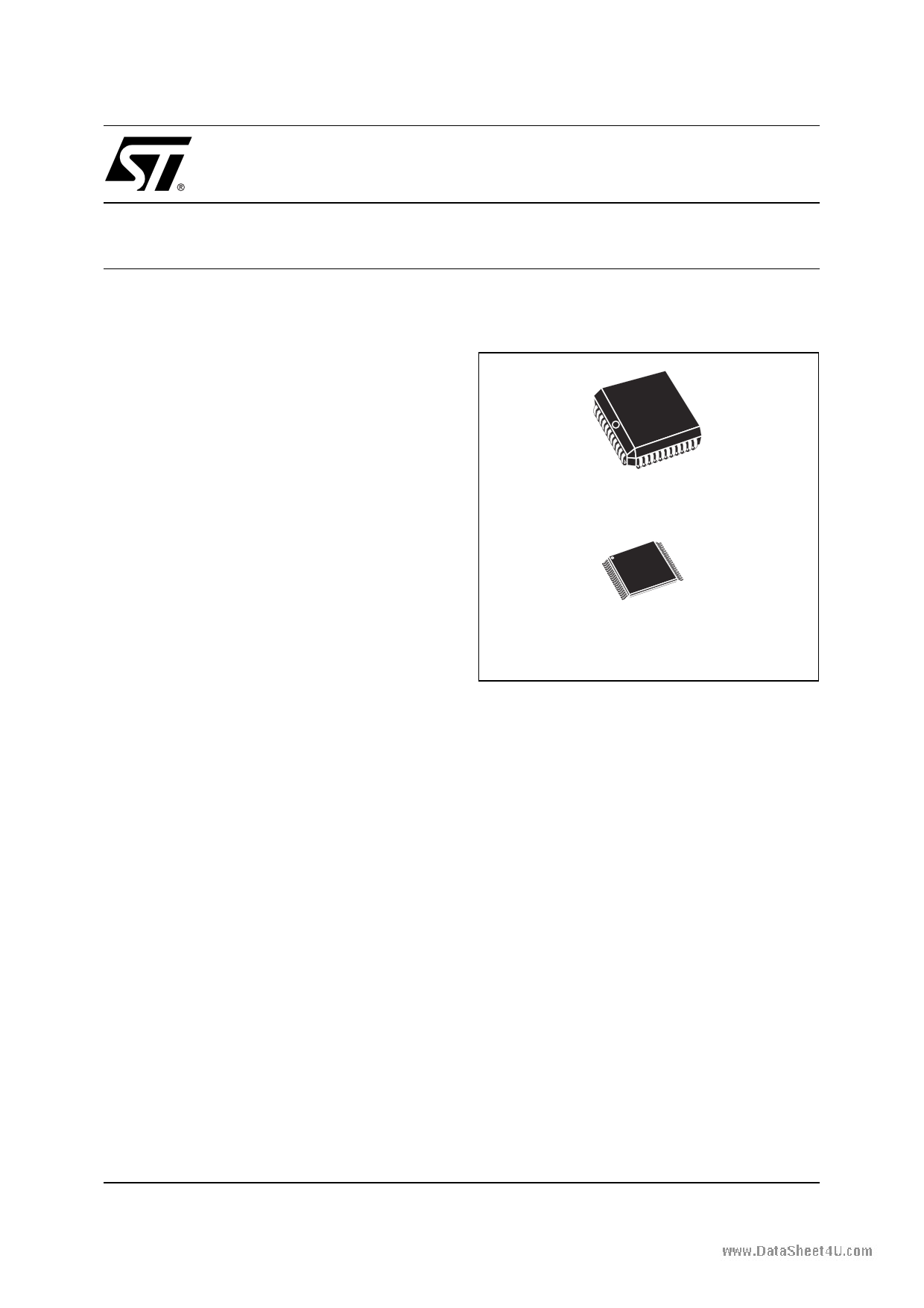
Figure 1. Package
PLCC44 (K)
TSOP40 (N)
10 x 14mm
November 2004
1/24
1 page 
www.DataSheet4U.com
Figure 3. PLCC Connections
DQ12
DQ11
DQ10
DQ9
DQ8
VSS
NC
DQ7
DQ6
DQ5
DQ4
12
1 44
M29F102BB
23
A13
A12
A11
A10
A9
34 VSS
NC
A8
A7
A6
A5
AI02131C
M29F102BB
Figure 4. TSOP Connections
A9
A10
A11
A12
A13
A14
A15
NC
W
VCC
RP
E
DQ15
DQ14
DQ13
DQ12
DQ11
DQ10
DQ9
DQ8
1 40
10 M29F102BB 31
11 30
20 21
AI02132C
VSS
A8
A7
A6
A5
A4
A3
A2
A1
A0
G
DQ0
DQ1
DQ2
DQ3
DQ4
DQ5
DQ6
DQ7
VSS
5/24
5 Page 
www.DataSheet4U.com
M29F102BB
STATUS REGISTER
Bus Read operations from any address always
read the Status Register during Program and
Erase operations. It is also read during Erase Sus-
pend when an address within a block being erased
is accessed.
The bits in the Status Register are summarized in
Table 6., Status Register Bits.
Data Polling Bit (DQ7). The Data Polling Bit can
be used to identify whether the Program/Erase
Controller has successfully completed its opera-
tion or if it has responded to an Erase Suspend.
The Data Polling Bit is output on DQ7 when the
Status Register is read.
During Program operations the Data Polling Bit
outputs the complement of the bit being pro-
grammed to DQ7. After successful completion of
the Program operation the memory returns to
Read mode and Bus Read operations from the ad-
dress just programmed output DQ7, not its com-
plement.
During Erase operations the Data Polling Bit out-
puts ’0’, the complement of the erased state of
DQ7. After successful completion of the Erase op-
eration the memory returns to Read Mode.
In Erase Suspend mode the Data Polling Bit will
output a ’1’ during a Bus Read operation within a
block being erased. The Data Polling Bit will
change from a ’0’ to a ’1’ when the Program/Erase
Controller has suspended the Erase operation.
Figure 5., Data Polling Flowchart, gives an exam-
ple of how to use the Data Polling Bit. A Valid Ad-
dress is the address being programmed or an
address within the block being erased.
Toggle Bit (DQ6). The Toggle Bit can be used to
identify whether the Program/Erase Controller has
successfully completed its operation or if it has re-
sponded to an Erase Suspend. The Toggle Bit is
output on DQ6 when the Status Register is read.
During Program and Erase operations the Toggle
Bit changes from ’0’ to ’1’ to ’0’, etc., with succes-
sive Bus Read operations at any address. After
successful completion of the operation the memo-
ry returns to Read mode.
During Erase Suspend mode the Toggle Bit will
output when addressing a cell within a block being
erased. The Toggle Bit will stop toggling when the
Program/Erase Controller has suspended the
Erase operation.
Figure 6., Data Toggle Flowchart, gives an exam-
ple of how to use the Data Toggle Bit.
Error Bit (DQ5). The Error Bit can be used to
identify errors detected by the Program/Erase
Controller. The Error Bit is set to ’1’ when a Pro-
gram, Block Erase or Chip Erase operation fails to
write the correct data to the memory. If the Error
Bit is set a Read/Reset command must be issued
before other commands are issued. The Error bit
is output on DQ5 when the Status Register is read.
Note that the Program command cannot change a
bit set at ’0’ back to ’1’ and attempting to do so may
or may not set DQ5 at ‘1’. In both cases, a succes-
sive Bus Read operation will show the bit is still ‘0’.
One of the Erase commands must be used to set
all the bits in a block or in the whole memory from
’0’ to ’1’.
Erase Timer Bit (DQ3). The Erase Timer Bit can
be used to identify the start of Program/Erase
Controller operation during a Block Erase com-
mand. Once the Program/Erase Controller starts
erasing the Erase Timer Bit is set to ’1’. Before the
Program/Erase Controller starts the Erase Timer
Bit is set to ’0’ and additional blocks to be erased
may be written to the Command Interface. The
Erase Timer Bit is output on DQ3 when the Status
Register is read.
Alternative Toggle Bit (DQ2). The Alternative
Toggle Bit can be used to monitor the Program/
Erase controller during Erase operations. The Al-
ternative Toggle Bit is output on DQ2 when the
Status Register is read.
During Chip Erase and Block Erase operations the
Toggle Bit changes from ’0’ to ’1’ to ’0’, etc., with
successive Bus Read operations from addresses
within the blocks being erased. Once the operation
completes the memory returns to Read mode.
During Erase Suspend the Alternative Toggle Bit
changes from ’0’ to ’1’ to ’0’, etc. with successive
Bus Read operations from addresses within the
blocks being erased. Bus Read operations to ad-
dresses within blocks not being erased will output
the memory cell data as if in Read mode.
After an Erase operation that causes the Error Bit
to be set the Alternative Toggle Bit can be used to
identify which block or blocks have caused the er-
ror. The Alternative Toggle Bit changes from ’0’ to
’1’ to ’0’, etc. with successive Bus Read Opera-
tions from addresses within blocks that have not
erased correctly. The Alternative Toggle Bit does
not change if the addressed block has erased cor-
rectly.
11/24
11 Page | ||
| Páginas | Total 24 Páginas | |
| PDF Descargar | [ Datasheet 29F102BB.PDF ] | |
Hoja de datos destacado
| Número de pieza | Descripción | Fabricantes |
| 29F102BB | MM29F102BB | ST Microelectronics |
| Número de pieza | Descripción | Fabricantes |
| SLA6805M | High Voltage 3 phase Motor Driver IC. |
Sanken |
| SDC1742 | 12- and 14-Bit Hybrid Synchro / Resolver-to-Digital Converters. |
Analog Devices |
|
DataSheet.es es una pagina web que funciona como un repositorio de manuales o hoja de datos de muchos de los productos más populares, |
| DataSheet.es | 2020 | Privacy Policy | Contacto | Buscar |