|
|
PDF MC74VHC1GT00 Data sheet ( Hoja de datos )
| Número de pieza | MC74VHC1GT00 | |
| Descripción | 2-Input NAND Gate/CMOS Logic Level Shifter | |
| Fabricantes | ON Semiconductor | |
| Logotipo | ||
Hay una vista previa y un enlace de descarga de MC74VHC1GT00 (archivo pdf) en la parte inferior de esta página. Total 8 Páginas | ||
|
No Preview Available !
MC74VHC1GT00
2-Input NAND Gate /
CMOS Logic Level Shifter
with LSTTL–Compatible Inputs
The MC74VHC1GT00 is a single gate 2–input NAND fabricated
with silicon gate CMOS technology. It achieves high speed operation
similar to equivalent Bipolar Schottky TTL while maintaining CMOS
low power dissipation.
The internal circuit is composed of three stages, including a buffer
output which provides high noise immunity and stable output.
The device input is compatible with TTL–type input thresholds and
the output has a full 5V CMOS level output swing. The input
protection circuitry on this device allows overvoltage tolerance on the
input, allowing the device to be used as a logic–level translator from
3.0V CMOS logic to 5.0V CMOS Logic or from 1.8V CMOS logic to
3.0V CMOS Logic while operating at the high–voltage power supply.
The MC74VHC1GT00 input structure provides protection when
voltages up to 7V are applied, regardless of the supply voltage. This
allows the MC74VHC1GT00 to be used to interface 5V circuits to 3V
circuits. The output structures also provide protection when VCC = 0V.
These input and output structures help prevent device destruction
caused by supply voltage – input/output voltage mismatch, battery
backup, hot insertion, etc.
• High Speed: tPD = 3.1ns (Typ) at VCC = 5V
• Low Power Dissipation: ICC = 2µA (Max) at TA = 25°C
• TTL–Compatible Inputs: VIL = 0.8V; VIH = 2.0V
• CMOS–Compatible Outputs: VOH > 0.8VCC; VOL < 0.1VCC @Load
• Power Down Protection Provided on Inputs and Outputs
• Balanced Propagation Delays
• Pin and Function Compatible with Other Standard Logic Families
• Latchup Performance Exceeds 300mA
• ESD Performance: HBM > 2000V
http://onsemi.com
SC–88A / SOT–353
DF SUFFIX
CASE 419A
MARKING DIAGRAM
VHd
Pin 1
d = Date Code
PIN ASSIGNMENT
1 IN B
2 IN A
3 GND
4 OUT Y
5 VCC
IN B 1
IN A 2
GND 3
5 VCC
4 OUT Y
Figure 1. 5–Lead SOT–353 Pinout (Top View)
LOGIC SYMBOL
IN A &
IN B OUT Y
ORDERING INFORMATION
See detailed ordering and shipping information in the package
dimensions section on page 4 of this data sheet.
FUNCTION TABLE
Inputs
AB
LL
LH
HL
HH
Output
Y
H
H
H
L
© Semiconductor Components Industries, LLC, 1999
December, 1999 – Rev. 2
1
Publication Order Number:
MC74VHC1GT00/D
1 page 
K
t
TOP
COVER
TAPE
B1 K0
SEE
NOTE 2
FOR MACHINE REFERENCE
ONLY
INCLUDING DRAFT AND RADII
CONCENTRIC AROUND B0
MC74VHC1GT00
10 PITCHES
CUMULATIVE
TOLERANCE ON
P0
TAPE
±0.2 mm
D P2 (±0.008”)
E
A0 SEE NOTE 2
+ B0
+
P
EMBOSSMENT
USER DIRECTION OF FEED
FW
+
CENTER LINES
OF CAVITY
D1
FOR COMPONENTS
2.0 mm × 1.2 mm
AND LARGER
BENDING RADIUS
R MIN.
TAPE AND COMPONENTS
SHALL PASS AROUND RADIUS “R”
WITHOUT DAMAGE
EMBOSSED
CARRIER
*TOP COVER
TAPE THICKNESS (t1)
0.10 mm
(0.004”) MAX.
EMBOSSMENT
MAXIMUM COMPONENT ROTATION
10°
TYPICAL
COMPONENT CAVITY
CENTER LINE
100 mm
(3.937”)
1 mm MAX
TAPE
TYPICAL
COMPONENT
CENTER LINE
1 mm
250 mm
(0.039”) MAX (9.843”)
CAMBER (TOP VIEW)
ALLOWABLE CAMBER TO BE 1 mm/100 mm NONACCUMULATIVE OVER 250 mm
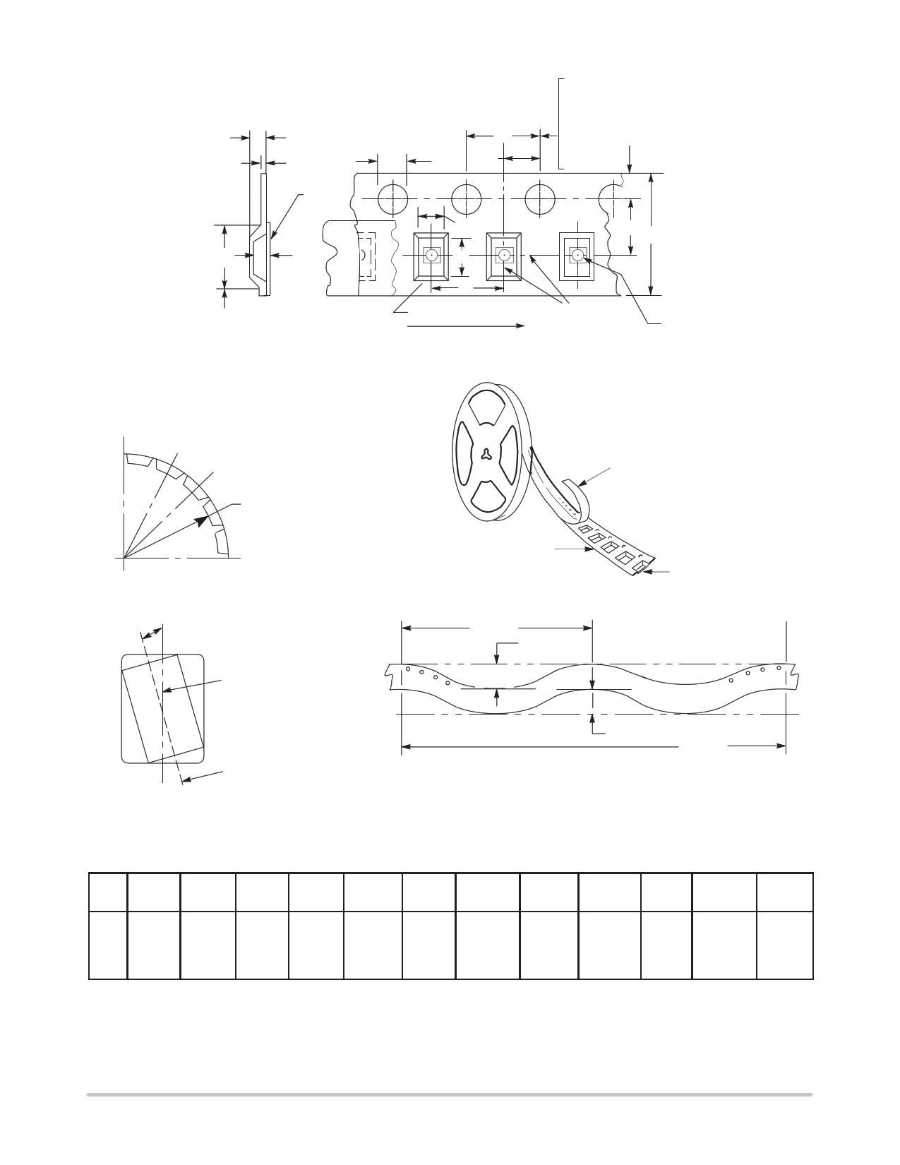
Figure 4. Carrier Tape Specifications
EMBOSSED CARRIER DIMENSIONS (See Notes 1 and 2)
Tape B1
Size Max
D
D1
E
F
K
P
P0 P2 R
T
W
8 mm 4.35 mm
(0.171”)
1.5 +0.1/
–0.0 mm
(0.059
+0.004/
–0.0”)
1.0 mm
Min
(0.039”)
1.75
±0.1 mm
(0.069
±0.004”)
3.5
±0.5 mm
(1.38
±0.002”)
2.4 mm
(0.094”)
4.0
±0.10 mm
(0.157
±0.004”)
4.0
±0.1 mm
(0.156
±0.004”)
2.0
±0.1 mm
(0.079
±0.002”)
25 mm
(0.98”)
0.3
±0.05 mm
(0.01
+0.0038/
–0.0002”)
8.0
±0.3 mm
(0.315
±0.012”)
1. Metric Dimensions Govern–English are in parentheses for reference only.
2. A0, B0, and K0 are determined by component size. The clearance between the components and the cavity must be within 0.05 mm min to
0.50 mm max. The component cannot rotate more than 10° within the determined cavity
http://onsemi.com
5
5 Page | ||
| Páginas | Total 8 Páginas | |
| PDF Descargar | [ Datasheet MC74VHC1GT00.PDF ] | |
Hoja de datos destacado
| Número de pieza | Descripción | Fabricantes |
| MC74VHC1GT00 | 2-Input NAND Gate/CMOS Logic Level Shifter | ON Semiconductor |
| MC74VHC1GT00 | 2-Input NAND Gate / CMOS Logic Level Shifter | ETL |
| MC74VHC1GT02 | 2-Input NOR Gate/CMOS Logic Level Shifter | ON Semiconductor |
| MC74VHC1GT02 | 2-Input NOR Gate / CMOS Logic Level Shifter | ETL |
| Número de pieza | Descripción | Fabricantes |
| SLA6805M | High Voltage 3 phase Motor Driver IC. |
Sanken |
| SDC1742 | 12- and 14-Bit Hybrid Synchro / Resolver-to-Digital Converters. |
Analog Devices |
|
DataSheet.es es una pagina web que funciona como un repositorio de manuales o hoja de datos de muchos de los productos más populares, |
| DataSheet.es | 2020 | Privacy Policy | Contacto | Buscar |
