|
|
|
PDF MVTX2801 Data sheet ( Hoja de datos )
| Número de pieza | MVTX2801 | |
| Descripción | Unmanaged 4-Port 1000 Mbps Ethernet Switch | |
| Fabricantes | Zarlink Semiconductor | |
| Logotipo | ||
Hay una vista previa y un enlace de descarga de MVTX2801 (archivo pdf) en la parte inferior de esta página. Total 30 Páginas | ||
|
No Preview Available !
Features
• 4 Gigabit Ports with GMII and PCS interface
- Gigabit Port can also support 100/10 Mbps MII
interface
• High Performance Layer 2 Packet Forwarding
(11.904M packets per second) and Filtering at
Full-Wire Speed
• Maximum throughput is 4 Gbps non-blocking
• Centralized shared-memory architecture
• Consists of two Memory Domains at 133 MHz
- Frame Buffer Domain: one bank of ZBT-SRAM
with 1M/2MB total
- Switch Database Domain with 256K/512K
SRAM.
• Up to 64K MAC addresses to provide large node
aggregation in wiring closet switches
Traffic Classification
• Classify traffic into 8 transmission priorities per
port
• Supports Delay bounded, Strict Priority, and WFQ
MVTX2801
Unmanaged 4-Port 1000 Mbps
Ethernet Switch
Data Sheet
October 2003
Ordering Information
MVTX2801AG 596-pin HSBGA
-40°C to +85°C
• Provides 2 level dropping precedence with WRED
mechanism
- User controlled thresholds for WRED
• Classification based on layer 2, 3 markings
- VLAN Priority field in VLAN tagged frame.
- DS/TOS field in IP packet
- The precedence of above two classifications
can be programmable
• QoS Support
• Supports IEEE 802.1p/Q Quality of Service with 8
Priority
• Buffer Management: reserve buffers on per class
and per port basis
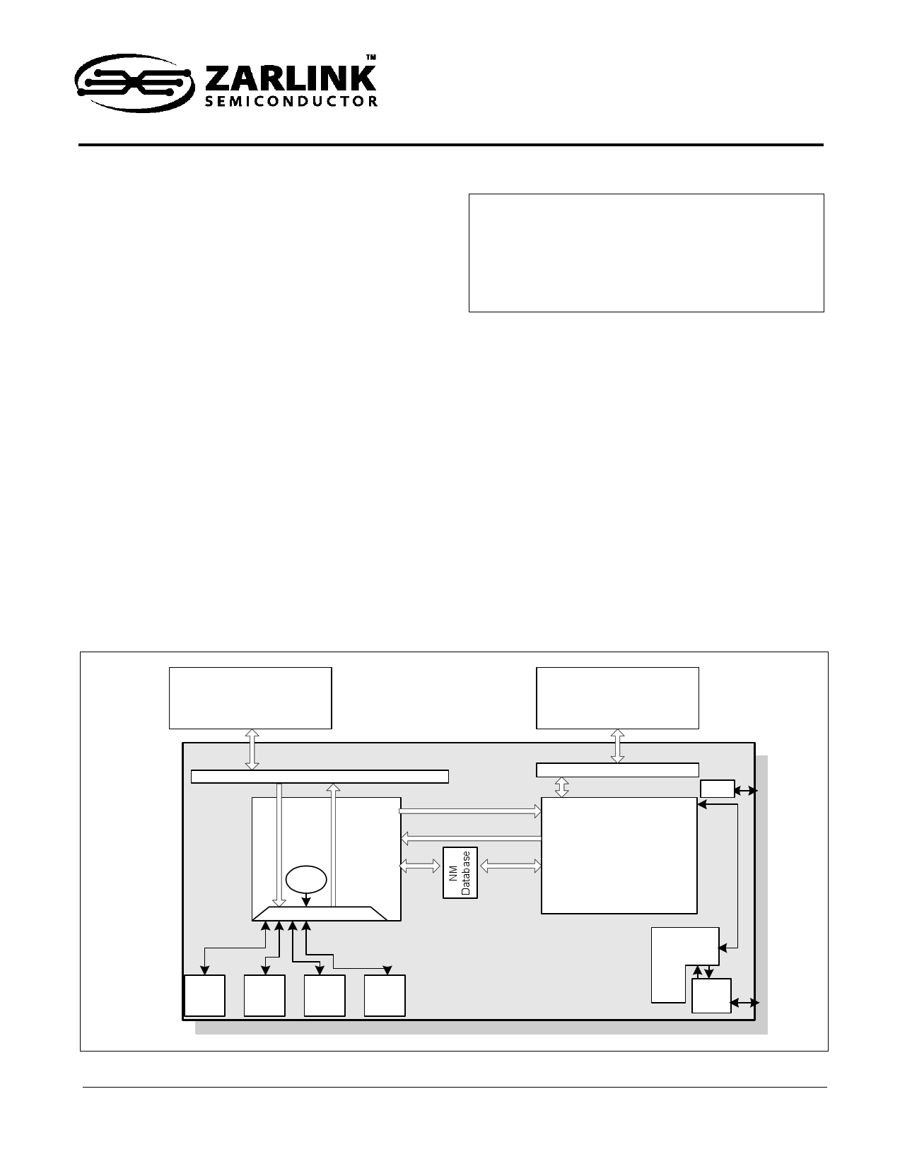
Frame Data Buffer A
ZBT-SRAM (1M/2MB)
VTX2800
64bit
FDB Interface
Frame
Engine
Scheduler
SRAM 256/512K
SW Databasee
MAC Table
32bit
SDB Interface
Search
Engine
LED
GMII
/PCS
Port 0
GMII
/PCS
Port 1
GMII
/PCS
Port 2
GMII
/PCS
Port 3
Management
Module
Serial /
I2C
Figure 1 - Chip Block Diagram
1
Zarlink Semiconductor Inc.
Zarlink, ZL and the Zarlink Semiconductor logo are trademarks of Zarlink Semiconductor Inc.
Copyright 2003, Zarlink Semiconductor Inc. All Rights Reserved.
1 page 
MVTX2801
Data Sheet
10.6.20 C5RS - Class 5 Reserved Size . . . . . . . . . . . . . . . . . . . . . . . . . . . . . . . . . . . . . . . . . . . . . . . . . . 45
10.6.21 C6RS - Class 6 Reserved Size . . . . . . . . . . . . . . . . . . . . . . . . . . . . . . . . . . . . . . . . . . . . . . . . . . 45
10.6.22 C7RS - Class 7 Reserved Size . . . . . . . . . . . . . . . . . . . . . . . . . . . . . . . . . . . . . . . . . . . . . . . . . . 46
10.6.23 QOSC00 - BYTE_C2_G0. . . . . . . . . . . . . . . . . . . . . . . . . . . . . . . . . . . . . . . . . . . . . . . . . . . . . . . 46
10.6.24 QOSC01 - BYTE_C3_G0. . . . . . . . . . . . . . . . . . . . . . . . . . . . . . . . . . . . . . . . . . . . . . . . . . . . . . . 46
10.6.25 QOSC02 - BYTE_C4_G0. . . . . . . . . . . . . . . . . . . . . . . . . . . . . . . . . . . . . . . . . . . . . . . . . . . . . . . 46
10.6.26 QOSC03 - BYTE_C5_G0. . . . . . . . . . . . . . . . . . . . . . . . . . . . . . . . . . . . . . . . . . . . . . . . . . . . . . . 46
10.6.27 QOSC04 - BYTE_C6_G0. . . . . . . . . . . . . . . . . . . . . . . . . . . . . . . . . . . . . . . . . . . . . . . . . . . . . . . 47
10.6.28 QOSC05 - BYTE_C7_G0. . . . . . . . . . . . . . . . . . . . . . . . . . . . . . . . . . . . . . . . . . . . . . . . . . . . . . . 47
10.6.29 QOSC06 - BYTE_C2_G1. . . . . . . . . . . . . . . . . . . . . . . . . . . . . . . . . . . . . . . . . . . . . . . . . . . . . . . 47
10.6.30 QOSC07 - BYTE_C3_G1 . . . . . . . . . . . . . . . . . . . . . . . . . . . . . . . . . . . . . . . . . . . . . . . . . . . . . . 47
10.6.31 QOSC08 - BYTE_C4_G1 . . . . . . . . . . . . . . . . . . . . . . . . . . . . . . . . . . . . . . . . . . . . . . . . . . . . . . 47
10.6.32 QOSC09 - BYTE_C5_G1 . . . . . . . . . . . . . . . . . . . . . . . . . . . . . . . . . . . . . . . . . . . . . . . . . . . . . . 47
10.6.33 QOSC0A - BYTE_C6_G1 . . . . . . . . . . . . . . . . . . . . . . . . . . . . . . . . . . . . . . . . . . . . . . . . . . . . . . 48
10.6.34 QOSC0B - BYTE_C7_G1 . . . . . . . . . . . . . . . . . . . . . . . . . . . . . . . . . . . . . . . . . . . . . . . . . . . . . . 48
10.6.35 QOSC0C - BYTE_C2_G2 . . . . . . . . . . . . . . . . . . . . . . . . . . . . . . . . . . . . . . . . . . . . . . . . . . . . . . 48
10.6.36 QOSC0D - BYTE_C3_G2 . . . . . . . . . . . . . . . . . . . . . . . . . . . . . . . . . . . . . . . . . . . . . . . . . . . . . . 48
10.6.37 QOSC0E - BYTE_C4_G2 . . . . . . . . . . . . . . . . . . . . . . . . . . . . . . . . . . . . . . . . . . . . . . . . . . . . . . 48
10.6.38 QOSC0F - BYTE_C5_G2 . . . . . . . . . . . . . . . . . . . . . . . . . . . . . . . . . . . . . . . . . . . . . . . . . . . . . . 49
10.6.39 QOSC10 - BYTE_C6_G2. . . . . . . . . . . . . . . . . . . . . . . . . . . . . . . . . . . . . . . . . . . . . . . . . . . . . . . 49
10.6.40 QOSC11 - BYTE_C7_G2. . . . . . . . . . . . . . . . . . . . . . . . . . . . . . . . . . . . . . . . . . . . . . . . . . . . . . . 49
10.6.41 QOSC12 - BYTE_C2_G3 . . . . . . . . . . . . . . . . . . . . . . . . . . . . . . . . . . . . . . . . . . . . . . . . . . . . . . 49
10.6.42 QOSC13 - BYTE_C3_G3. . . . . . . . . . . . . . . . . . . . . . . . . . . . . . . . . . . . . . . . . . . . . . . . . . . . . . . 49
10.6.44 QOSC15 - BYTE_C5_G3. . . . . . . . . . . . . . . . . . . . . . . . . . . . . . . . . . . . . . . . . . . . . . . . . . . . . . . 50
10.6.45 QOSC16 - BYTE_C6_G3 . . . . . . . . . . . . . . . . . . . . . . . . . . . . . . . . . . . . . . . . . . . . . . . . . . . . . . 50
10.6.46 QOSC17 - BYTE_C7_G3. . . . . . . . . . . . . . . . . . . . . . . . . . . . . . . . . . . . . . . . . . . . . . . . . . . . . . . 50
10.6.47 QOSC33 - CREDIT_C0_G0. . . . . . . . . . . . . . . . . . . . . . . . . . . . . . . . . . . . . . . . . . . . . . . . . . . . . 50
10.6.48 QOSC34 - CREDIT_C1_G0. . . . . . . . . . . . . . . . . . . . . . . . . . . . . . . . . . . . . . . . . . . . . . . . . . . . . 51
10.6.49 QOSC35 - CREDIT_C2_G0. . . . . . . . . . . . . . . . . . . . . . . . . . . . . . . . . . . . . . . . . . . . . . . . . . . . . 51
10.6.50 QOSC36 - CREDIT_C3_G0 . . . . . . . . . . . . . . . . . . . . . . . . . . . . . . . . . . . . . . . . . . . . . . . . . . . . 51
10.6.51 QOSC37 - CREDIT_C4_G0. . . . . . . . . . . . . . . . . . . . . . . . . . . . . . . . . . . . . . . . . . . . . . . . . . . . . 51
10.6.52 QOSC38 - CREDIT_C5_G0. . . . . . . . . . . . . . . . . . . . . . . . . . . . . . . . . . . . . . . . . . . . . . . . . . . . . 52
10.6.53 QOSC39- CREDIT_C6_G0 . . . . . . . . . . . . . . . . . . . . . . . . . . . . . . . . . . . . . . . . . . . . . . . . . . . . . 52
10.6.54 QOSC3A- CREDIT_C7_G0 . . . . . . . . . . . . . . . . . . . . . . . . . . . . . . . . . . . . . . . . . . . . . . . . . . . . . 52
10.6.55 QOSC3B - CREDIT_C0_G1 . . . . . . . . . . . . . . . . . . . . . . . . . . . . . . . . . . . . . . . . . . . . . . . . . . . . 52
10.6.56 QOSC3C - CREDIT_C1_G1 . . . . . . . . . . . . . . . . . . . . . . . . . . . . . . . . . . . . . . . . . . . . . . . . . . . . 53
10.6.57 QOSC3D - CREDIT_C2_G1 . . . . . . . . . . . . . . . . . . . . . . . . . . . . . . . . . . . . . . . . . . . . . . . . . . . . 53
10.6.58 QOSC3E - CREDIT_C3_G1 . . . . . . . . . . . . . . . . . . . . . . . . . . . . . . . . . . . . . . . . . . . . . . . . . . . . 53
10.6.59 QOSC3F - CREDIT_C4_G1 . . . . . . . . . . . . . . . . . . . . . . . . . . . . . . . . . . . . . . . . . . . . . . . . . . . . 53
10.6.60 QOSC40 - CREDIT_C5_G1. . . . . . . . . . . . . . . . . . . . . . . . . . . . . . . . . . . . . . . . . . . . . . . . . . . . . 54
10.6.61 QOSC41- CREDIT_C6_G1 . . . . . . . . . . . . . . . . . . . . . . . . . . . . . . . . . . . . . . . . . . . . . . . . . . . . . 54
10.6.62 QOSC42- CREDIT_C7_G1 . . . . . . . . . . . . . . . . . . . . . . . . . . . . . . . . . . . . . . . . . . . . . . . . . . . . . 54
10.6.63 QOSC43 - CREDIT_C0_G2 . . . . . . . . . . . . . . . . . . . . . . . . . . . . . . . . . . . . . . . . . . . . . . . . . . . . 54
10.6.64 QOSC44 - CREDIT_C1_G2 . . . . . . . . . . . . . . . . . . . . . . . . . . . . . . . . . . . . . . . . . . . . . . . . . . . . 55
10.6.65 QOSC45 - CREDIT_C2_G2. . . . . . . . . . . . . . . . . . . . . . . . . . . . . . . . . . . . . . . . . . . . . . . . . . . . . 55
10.6.66 QOSC46 - CREDIT_C3_G2 . . . . . . . . . . . . . . . . . . . . . . . . . . . . . . . . . . . . . . . . . . . . . . . . . . . . 55
10.6.67 QOSC47 - CREDIT_C4_G2. . . . . . . . . . . . . . . . . . . . . . . . . . . . . . . . . . . . . . . . . . . . . . . . . . . . . 55
10.6.68 QOSC48 - CREDIT_C5_G2 . . . . . . . . . . . . . . . . . . . . . . . . . . . . . . . . . . . . . . . . . . . . . . . . . . . . 56
10.6.69 QOSC49- CREDIT_C6_G2 . . . . . . . . . . . . . . . . . . . . . . . . . . . . . . . . . . . . . . . . . . . . . . . . . . . . . 56
10.6.70 QOSC4A- CREDIT_C7_G2 . . . . . . . . . . . . . . . . . . . . . . . . . . . . . . . . . . . . . . . . . . . . . . . . . . . . . 56
10.6.71 QOSC4B - CREDIT_C0_G3 . . . . . . . . . . . . . . . . . . . . . . . . . . . . . . . . . . . . . . . . . . . . . . . . . . . . 56
10.6.72 QOSC4 - CREDIT_C1_G3. . . . . . . . . . . . . . . . . . . . . . . . . . . . . . . . . . . . . . . . . . . . . . . . . . . . . . 57
10.6.73 QOSC4D - CREDIT_C2_G3 . . . . . . . . . . . . . . . . . . . . . . . . . . . . . . . . . . . . . . . . . . . . . . . . . . . . 57
10.6.74 QOSC4E - CREDIT_C3_G3 . . . . . . . . . . . . . . . . . . . . . . . . . . . . . . . . . . . . . . . . . . . . . . . . . . . . 57
5
Zarlink Semiconductor Inc.
5 Page 
MVTX2801
Data Sheet
2.0 System Configuration
The MVTX2801 can be configured by EEPROM (24C02 or compatible) via an I2C interface at boot time, or via a
synchronous serial interface during operation.
2.1 I2C Interface
The I2C interface uses two bus lines, a serial data line (SDA) and a serial clock line (SCL). The SCL line carries the
control signals that facilitate the transfer of information from EEPROM to the switch. Data transfer is 8-bit serial and
bi-directional, at 50 Kbps. Data transfer is performed between master and slave IC using a request /
acknowledgment style of protocol. The master IC generates the timing signals and terminates data transfer. The
figure below shows the data transfer format.
START
SLAVE
ADDRESS
R/W ACK
DATA 1
(8 bits)
ACK
DATA 2
ACK
DATA M
Figure 2 - Data Transfer Format for I2C Interface
ACK
STOP
2.1.1 Start Condition
Generated by the master, the MVTX2801. The bus is considered to be busy after the Start condition is generated.
The Start condition occurs if while the SCL line is High, there is a High-to-Low transition of the SDA line.
Other than in the Start condition (and Stop condition), the data on the SDA line must be stable during the High period
of SCL. The High or Low state of SDA can only change when SCL is Low. In addition, when the I2C bus is free, both
lines are High.
2.1.2 Address
The first byte after the Start condition determines which slave the master will select. The slave in our case is the
EEPROM. The first seven bits of the first data byte make up the slave address.
2.1.3 Data Direction
The eighth bit in the first byte after the Start condition determines the direction (R/W) of the message. A master
transmitter sets this bit to W; a master receiver sets this bit to R.
2.1.4 Acknowledgment
Like all clock pulses, the master generates the acknowledgment-related clock pulse. However, the transmitter
releases the SDA line (High) during the acknowledgment clock pulse. Furthermore, the receiver must pull down the
SDA line during the acknowledge pulse so that it remains stable Low during the High period of this clock pulse. An
acknowledgment pulse follows every byte transfer.
If a slave receiver does not acknowledge after any byte, then the master generates a Stop condition and aborts the
transfer.
If a master receiver does not acknowledge after any byte, then the slave transmitter must release the SDA line to let
the master generate the Stop condition.
2.1.5 Data
After the first byte containing the address, all bytes that follow are data bytes. Each byte must be followed by an
acknowledge bit. Data is transferred MSB-first.
11
Zarlink Semiconductor Inc.
11 Page | ||
| Páginas | Total 30 Páginas | |
| PDF Descargar | [ Datasheet MVTX2801.PDF ] | |
Hoja de datos destacado
| Número de pieza | Descripción | Fabricantes |
| MVTX2801 | Unmanaged 4-Port 1000 Mbps Ethernet Switch | Zarlink Semiconductor |
| MVTX2802 | Managed 4-Port 1000 Mbps Ethernet Switch | Zarlink Semiconductor |
| MVTX2803 | Unmanaged 8-Port 1000 Mbps Ethernet Switch | Zarlink Semiconductor |
| MVTX2804 | 8-Port 1000 Mbps Ethernet Distributed Switch | Zarlink Semiconductor |
| Número de pieza | Descripción | Fabricantes |
| SLA6805M | High Voltage 3 phase Motor Driver IC. |
Sanken |
| SDC1742 | 12- and 14-Bit Hybrid Synchro / Resolver-to-Digital Converters. |
Analog Devices |
|
DataSheet.es es una pagina web que funciona como un repositorio de manuales o hoja de datos de muchos de los productos más populares, |
| DataSheet.es | 2020 | Privacy Policy | Contacto | Buscar |