|
|
|
PDF SY100E195 Data sheet ( Hoja de datos )
| Número de pieza | SY100E195 | |
| Descripción | PROGRAMMABLE DELAY CHIP | |
| Fabricantes | Micrel Semiconductor | |
| Logotipo | ||
Hay una vista previa y un enlace de descarga de SY100E195 (archivo pdf) en la parte inferior de esta página. Total 8 Páginas | ||
|
No Preview Available !
PROGRAMMABLE
DELAY CHIP
ClockWorks™
SY10E195
SY100E195
FEATURES
s Up to 2ns delay range
s Extended 100E VEE range of –4.2V to –5.5V
s ≈20ps/digital step resolution
s >1GHz bandwidth
s On-chip cascade circuitry
s 75KkΩ input pulldown resistor
s Fully compatible with Motorola MC10E/100E195
s Available in 28-pin PLCC package
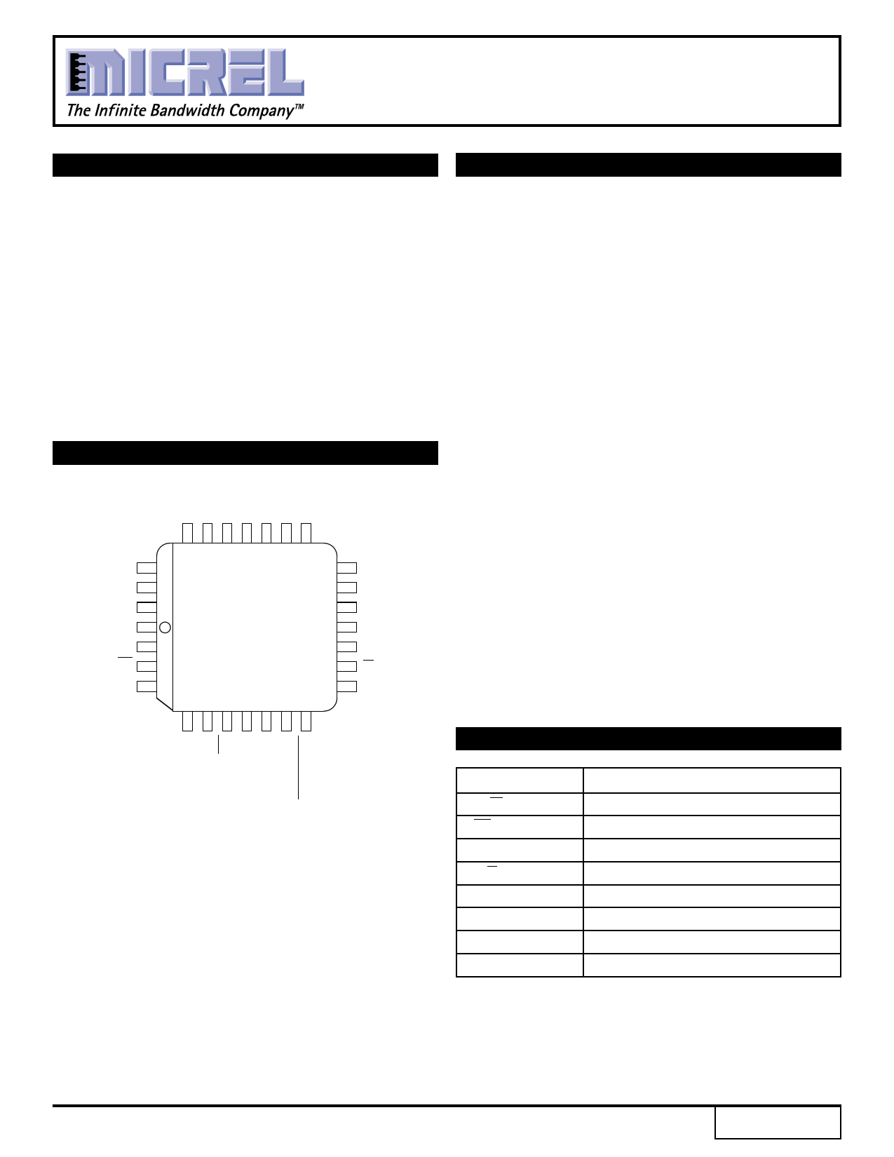
PIN CONFIGURATION
D1
D0
LEN
VEE
IN
IN
VBB
25 24 23 22 21 20 19
26 18
27 17
28 TOP VIEW 16
1
PLCC
15
2
J28-1
14
3 13
4 12
5 6 7 8 9 10 11
NC
NC
VCC
VCCO
Q
Q
VCCO
DESCRIPTION
The SY10/100E195 are programmable delay chips
(PDCs) designed primarily for clock de-skewing and timing
adjustment. They provide variable delay of a differential
ECL input transition.
The delay section consists of a chain of gates
organized as shown in the logic diagram. The first two
delay elements feature gates that have been modified to
have delays 1.25 and 1.5 times the basic gate delay of
approximately 80ps. These two elements provide the
E195 with a digitally-selectable resolution of
approximately 20ps. The required device delay is selected
by the seven address inputs D[0:6], which are latched
on-chip by a high signal on the latch enable (LEN) control.
If the LEN signal is either LOW or left floating, then the
latch is transparent.
Because the delay programmability of the E195 is
achieved by purely differential ECL gate delays, the
device will operate at frequencies of >1GHz, while
maintaining over 600mV of output swing.
The E195 thus offers very fine resolution, at very high
frequencies, selectable entirely from a digital input,
allowing for very accurate system clock timing.
An eighth latched input, D7, is provided for cascading
multiple PDCs for increased programmable range. The
cascade logic allows full control of multiple PDCs, at the
expense of only a single added line to the data bus for
each additional PDC, without the need for any external
gating.
PIN NAMES
Pin
IN/IN
EN
D[0:7]
Q/Q
LEN
SET MIN
SET MAX
CASCADE
Function
Signal Input
Input Enable
Mux Select Inputs
Signal Output
Latch Enable
Minimum Delay Set
Maximum Delay Set
Cascade Signal
Rev.: E Amendment: /0
1 Issue Date: October, 1998
1 page 
Micrel
APPLICATIONS INFORMATION
ADDRESS BUS (A0 – A6)
A7
ClockWorks™
SY10E195
SY100E195
Input
D1
D0
LEN
VEE
IN
IN
VBB
E196
Chip #1
VCC
VCCO
Q
Q
VCCO
D1
D0
LEN
VEE
IN
IN
VBB
E196
Chip #2
VCC
VCCO
Q
Q
VCCO
Output
Figure 1. Cascading Interconnect Architecture
Cascading Multiple E195s
To increase the programmable range of the E195,
internal cascade circuitry has been included. This circuitry
allows for the cascading of multiple E195s without the
need for any external gating. Furthermore, this capability
requires only one more address line per added E195.
Obviously, cascading multiple PDCs will result in a larger
programmable range; however, this increase is at the
expense of a longer minimum delay.
Figure 1 illustrates the interconnect scheme for
cascading two E195s. As can be seen, this scheme can
easily be expanded for larger E195 chains. The D7 input
of the E195 is the cascade control pin. With the
interconnect scheme of Figure 1, when D7 is asserted, it
signals the need for a larger programmable range than
is achievable with a single device.
An expansion of the latch section of the block diagram
is pictured below. Use of this diagram will simplify the
explanation of how the cascade circuitry works. When
D7 of chip #1 above is low, the cascade output will also
be low, while the cascade bar output will be a logical
high. In this condition, the SET MIN pin of chip #2 will
be asserted and, thus, all of the latches of chip #2 will
be reset and the device will be set at its minimum delay.
Since the RESET and SET inputs of the latches are
overriding, any changes on the A0–A6 address bus will
not affect the operation of chip #2.
Chip #1, on the other hand, will have both SET MIN
and SET MAX de-asserted so that its delay will be
controlled entirely by the address bus A0–A6. If the delay
needed is greater than can be achieved with 31.75 gate
delays (1111111 on the A0–A6 address bus), D7 will be
asserted to signal the need to cascade the delay to the
next E195 device. When D7 is asserted, the SET MIN
pin of chip #2 will be de-asserted and the delay will be
controlled by the A0–A6 address bus. Chip #1, on the
other hand, will have its SET MAX pin asserted, resulting
in the device delay to be independent of the A0–A6
address bus.
When the SET MAX pin of chip #1 is asserted, the D0
and D1 latches will be reset while the rest of the latches
will be set. In addition, to maintain monotonicity, an
additional gate delay is selected in the cascade circuitry.
As a result, when D7 of chip #1 is asserted, the delay
increases from 31.75 gates to 32 gates. A 32-gate delay
is the maximum delay setting for the E195.
To expand this cascading scheme to more devices,
one simply needs to connect the D7 input and CASCADE
outputs of the current most significant E195 to the new
most significant E195 in the same manner as pictured in
Figure 1. The only addition to the logic is the increase
of one line to the address bus for cascade control of the
second PDC.
5
5 Page | ||
| Páginas | Total 8 Páginas | |
| PDF Descargar | [ Datasheet SY100E195.PDF ] | |
Hoja de datos destacado
| Número de pieza | Descripción | Fabricantes |
| SY100E193 | ERROR DETECTION/ CORRECTION CIRCUIT | Micrel Semiconductor |
| SY100E195 | PROGRAMMABLE DELAY CHIP | Micrel Semiconductor |
| SY100E196 | PROGRAMMABLE DELAY CHIP WITH ANALOG INPUT | Micrel Semiconductor |
| Número de pieza | Descripción | Fabricantes |
| SLA6805M | High Voltage 3 phase Motor Driver IC. |
Sanken |
| SDC1742 | 12- and 14-Bit Hybrid Synchro / Resolver-to-Digital Converters. |
Analog Devices |
|
DataSheet.es es una pagina web que funciona como un repositorio de manuales o hoja de datos de muchos de los productos más populares, |
| DataSheet.es | 2020 | Privacy Policy | Contacto | Buscar |