|
|
|
PDF ICS950901 Data sheet ( Hoja de datos )
| Número de pieza | ICS950901 | |
| Descripción | Programmable Timing Control Hub | |
| Fabricantes | Integrated Circuit Systems | |
| Logotipo | ||
Hay una vista previa y un enlace de descarga de ICS950901 (archivo pdf) en la parte inferior de esta página. Total 20 Páginas | ||
|
No Preview Available !
Integrated
Circuit
Systems, Inc.
ICS950901
Programmable Timing Control Hub™ for P4™
Recommended Application:
VIA P4X266 chipset with PC133 or DDR memory.
Output Features:
• 2 - Pair of differential CPU clocks @ 3.3V
• 1 - Pair of differential push pull CPU_CS clocks @ 2.5V
• 3 - AGP @ 3.3V
• 9 - PCI @ 3.3V
• 2 - IOAPIC @ 2.5V
• 1 - 48MHz @ 3.3V fixed
• 1 - 24_48MHz @ 3.3V
• 1 - REF @ 3.3V, 14.318MHz
Features/Benefits:
• Programmable output frequency.
• Programmable output divider ratios.
• Programmable output rise/fall time.
• Programmable output skew.
• Programmable spread percentage for EMI control.
• Watchdog timer technology to reset system
if system malfunctions.
• Programmable watch dog safe frequency.
• Support I2C Index read/write and block read/write
operations.
• For DDR and or PC133 SDRAM system use ICS93718
as the memory buffer.
• Uses external 14.318MHz crystal.
Key Specifications:
• CPU_CS - CPU0: <±250ps
• CPU_CS - AGP: <±250ps
• PCI - PCI: <500ps
• CPU - PCI: Min = 1.0ns, Typ = 2.0ns, Max = 4.0ns
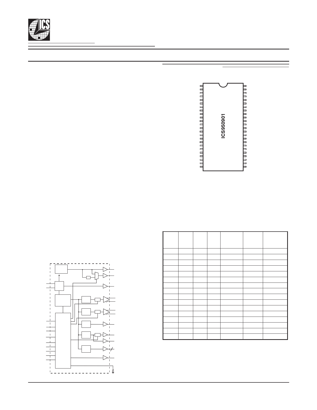
Block Diagram
PLL2
X1 XTAL
X2 OSC
PLL1
Spread
Spectrum
SEL24_48
SDATA
SCLK
FS (3:0)
PD#
PCI_STOP#
CPU_STOP#
MULTI_SEL
Vtt_PWRGD#
Control
Logic
Config.
Reg.
/2
CPU
DIVDER
Stop
CPU
DIVDER
Stop
IOAPIC
DIVDER
PCI
DIVDER
Stop
AGP
DIVDER
48MHz
24_48MHz
REF
CPUCLKT_(1:0)
CPUCLKC_(1:0)
CPUCLKT_CS
CPUCLKC_CS
IOAPIC (1:0)
PCICLK (7:0)
PCICLK_F
AGPCLK (2:0)
3
RESET#
I REF
Pin Configuration
1
*SEL24_48/REF
VDDREF
GND
X1
X2
VDD48
**FS3/48MHz
**FS2/24_48MHz
GND
*FS0/PCICLK_F
**FS1/PCICLK0
PCICLK1
GND
PCICLK2
PCICLK3
VDDPCI
PCICLK4
PCICLK5
PCICLK6
GND
PCICLK7
*PD#
AGPCLK0
VDDAGP
1
2
3
4
5
6
7
8
9
10
11
12
13
14
15
16
17
18
19
20
21
22
23
24
48 VDDAPIC (2.5V)
47 GND
46 IOAPIC0
45 IOAPIC1
44 GND
43 VDDCPU_CS (2.5V)
42 CPUCLKT_CS
41 CPUCLKC_CS
40 CPUCLKT_0
39 CPUCLKC_0
38 VDDCPU (3.3V)
37 I REF
36 GND
35 CPUCLKT_1
34 CPUCLKC_1
33 Vtt_PWRGD#
32 CPU_STOP#*
31 PCI_STOP#*
30 RESET#
29 SDATA
28 SCLK
27 AGPCLK2
26 AGPCLK1
25 GND
48-Pin 300-mil SSOP
1. These outputs have 2X drive strength.
* These inputs have a internal Pull-up resistor
of 120K to VDD
** These inputs have a internal pull-down to GND
Frequency Table
FS3
0
0
0
0
0
0
0
0
1
1
1
1
1
1
1
1
FS2
0
0
0
0
1
1
1
1
0
0
0
0
1
1
1
1
FS1
FS0
CPUCLK
MHz
0 0 66.67
0 1 100.00
1 0 133.33
1 1 200.00
0 0 100.90
0 1 103.00
1 0 107.00
1 1 110.00
0 0 133.90
0 1 137.33
1 0 140.00
1 1 142.66
0 0 145.33
0 1 146.66
1 0 153.33
1 1 160.00
AGP
MHz
66.66
66.67
66.67
66.66
67.27
68.67
71.33
73.33
66.95
68.66
70.00
71.33
72.66
73.33
76.66
80.00
PCICLK
MHz
33.33
33.33
33.33
33.33
33.63
34.33
35.67
36.67
33.48
34.33
35.00
35.67
36.33
36.67
38.33
40.00
0474F—05/25/05
1 page 
Integrated
Circuit
Systems, Inc.
Byte 1: CPU Active/Inactive Register
(1 = enable, 0 = disable)
Bit Pin# PWD
Description
Bit7 -
1 (Reserved)
Bit6 10
1 PCICLK_F (Active/Inactive)
Bit5 -
1 (Reserved)
Bit4 -
0 (Reserved)
Bit3 -
0 (Reserved)
Bit2 35, 34
1 CPUCLKT/C1 (Active/Inactive)
Bit1 40, 39
1 CPUCLKT/C0 (Active/Inactive)
Bit0 42, 41
1 CPUCLKT/C_CS (Active/Inactive)
Byte 2: PCI Active/Inactive Register
(1 = enable, 0 = disable)
Bit Pin# PWD
Bit7 21
1 PCICLK7 (Active/Inactive)
Bit6 19
1 PCICLK6 (Active/Inactive)
Bit5 18
1 PCICLK5 (Active/Inactive)
Bit4 17
1 PCICLK4 (Active/Inactive)
Bit3 15
1 PCICLK3 (Active/Inactive)
Bit2 14
1 PCICLK2 (Active/Inactive)
Bit1 12
1 PCICLK1 (Active/Inactive)
Bit0 11
1 PCICLK0 (Active/Inactive)
Description
Byte 3: Active/Inactive Register
(1 = enable, 0 = disable)
Bit Pin# PWD
Description
Bit7 -
1 Reserved
Bit6 1
1 SEL 24_48, 0=24Mhz 1=48MHz
Bit5 -
1 (Reserved)
Bit4 46
1 IOAPIC 0
Bit3 45
1 IOAPIC 1
Bit2 23
1 AGPCLK 0
Bit1 26
1 AGPCLK 1
Bit0 27
1 AGPCLK 2
Byte 4: Frequency Select Active/Inactive Register
(1 = enable, 0 = disable)
Bit
Bit 7
Bit 6
Bit 5
Bit 4
Bit 3
Bit 2
Bit 1
Bit 0
Pin#
-
-
-
-
7
8
-
1
PWD
X
X
X
X
1
1
0
1
Latched FS3#
Latched FS2#
Latched FS1#
Latched FS0#
48MHz (Active/Inactive)
24_48MHz (Active/Inactive)
Reserved
REF (Active/Inactive)
Description
Third party brands and names are the property of their respective owners.
5
ICS950901
5 Page 
Integrated
Circuit
Systems, Inc.
ICS950901
Absolute Maximum Ratings
Supply Voltage . . . . . . . . . . . . . . . . . . . . . . . . . . . . . . . . 5.5 V
Logic Inputs . . . . . . . . . . . . . . . . . . . . . . . . . . . . . . . . . . GND –0.5 V to VDD +0.5 V
Ambient Operating Temperature . . . . . . . . . . . . . . . . . 0°C to +70°C
Case Temperature . . . . . . . . . . . . . . . . . . . . . . . . . . . . . 115°C
Storage Temperature . . . . . . . . . . . . . . . . . . . . . . . . . . . –65°C to +150°C
Stresses above those listed under Absolute Maximum Ratings may cause permanent damage to the device. These ratings are
stress specifications only and functional operation of the device at these or any other conditions above those listed in the
operational sections of the specifications is not implied. Exposure to absolute maximum rating conditions for extended
periods may affect product reliability.
Electrical Characteristics - Input/Supply/Common Output Parameters.
TA = 0 - 70C; Supply Voltage VDD = 3.3 V + - 5% (unless otherwise stated)
PARAMETER SYMBOL
CONDITIONS
Input High Voltage
Input Low Voltage
Input High Current
Input Low Current
Input Low Current
Operating
Supply Current
Power Down
Supply Current
Input frequency
Pin Inductance
Input Capacitance1
Transition Time1
Settling Time1
Clk Stabilization1
Delay
Vih
Vil
Iih
Iil1
IIL2
IDD3.3OP
IDD3.3PD
Fi
Lpin
CIN
Cout
CINX
Ttrans
Ts
TSTAB
tPZH,tPZH
tPLZ,tPZH
Vin = VDD
Vin = 0 V; Inputs with no pull-up resistors
Vin = 0 V; Inputs with no pull-up resistors
Cl = 0 pF; Select @ 66M
Cl = Full load @ 133.3 MHz
IREF=2.32mA
IREF= 5mA
VDD = 3.3 V;
Logic Inputs
Output pin capacitance
X1 & X2 pins
To 1st crossing of target Freq.
From 1st crossing to 1% target Freq.
From VDD = 3.3V to 1% target Freq.
output enable delay (all outputs)
output disable delay (all outputs)
1 Guarenteed by design, not 100% tested in production.
MIN
2
VSS-0.3
-5
-5
-200
27
1
1
TYP
181
13
MAX
VDD+0.3
0.8
5
100
280
20
37
7
5
6
45
3
3
3
10
10
UNITS
V
V
mA
mA
mA
mA
mA
mA
mA
MHz
nH
pF
pF
pF
ms
ms
ms
ns
ns
Third party brands and names are the property of their respective owners.
11
11 Page | ||
| Páginas | Total 20 Páginas | |
| PDF Descargar | [ Datasheet ICS950901.PDF ] | |
Hoja de datos destacado
| Número de pieza | Descripción | Fabricantes |
| ICS950901 | Programmable Timing Control Hub | Integrated Circuit Systems |
| ICS950902 | Programmable Timing Control Hub | Integrated Circuit Systems |
| ICS950905 | Programmable Timing Control Hub | Integrated Circuit Systems |
| ICS950908 | Programmable Timing Control Hub | Integrated Circuit Systems |
| Número de pieza | Descripción | Fabricantes |
| SLA6805M | High Voltage 3 phase Motor Driver IC. |
Sanken |
| SDC1742 | 12- and 14-Bit Hybrid Synchro / Resolver-to-Digital Converters. |
Analog Devices |
|
DataSheet.es es una pagina web que funciona como un repositorio de manuales o hoja de datos de muchos de los productos más populares, |
| DataSheet.es | 2020 | Privacy Policy | Contacto | Buscar |