|
|
|
PDF LT1507CN8 Data sheet ( Hoja de datos )
| Número de pieza | LT1507CN8 | |
| Descripción | 500kHz Monolithic Buck Mode Switching Regulator | |
| Fabricantes | Linear Technology | |
| Logotipo | ||
Hay una vista previa y un enlace de descarga de LT1507CN8 (archivo pdf) en la parte inferior de esta página. Total 20 Páginas | ||
|
No Preview Available !
LT1507
500kHz Monolithic
Buck Mode Switching Regulator
FEATURES
s Constant 500kHz Switching Frequency
s Uses All Surface Mount Components
s Operates with Inputs as Low as 4V
s Saturated Switch Design (0.3Ω)
s Cycle-by-Cycle Current Limiting
s Easily Synchronizable
s Inductor Size as Low as 2µH
s Shutdown Current: 20µA
U
APPLICATIONS
s Portable Computers
s Battery-Powered Systems
s Battery Charger
s Distributed Power
DESCRIPTION
The LT®1507 is a 500kHz monolithic buck mode switching
regulator, functionally identical to the LT1375 but opti-
mized for lower input voltage applications. It will operate
over a 4V to 15V input range, compared with 5.5V to 25V
for the LT1375. A 1.5A switch is included on the die along
with all the necessary oscillator, control and logic cir-
cuitry. High switching frequency allows a considerable
reduction in the size of external components. The topology
is current mode for fast transient response and good loop
stability. Both fixed output voltage (3.3V) and adjustable
parts are available.
A special high speed bipolar process and new design
techniques allow this regulator to achieve high efficiency
at a high switching frequency. Efficiency is maintained
over a wide output current range by keeping quiescent
supply current to 4mA and by utilizing a supply boost
capacitor to allow the NPN power switch to saturate. A
shutdown signal will reduce supply current to 20µA. The
LT1507 can be externally synchronized from 570kHz to
1MHz with logic level inputs.
The LT1507 fits into standard 8-pin SO and PDIP pack-
ages. Temperature rise is kept to a minimum by the high
efficiency design. Full cycle-by-cycle short-circuit protec-
tion and thermal shutdown are provided. Standard surface
mount external parts are used including the inductor and
capacitors.
, LTC and LT are registered trademarks of Linear Technology Corporation.
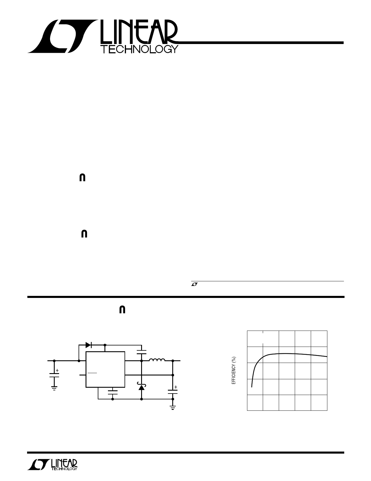
TYPICAL APPLICATION
5V to 3.3V Volt Down Converter
D2†
1N914
5V
C3*
47µF
16V
TANTALUM
+ DEFAULT
(OPEN)
= ON
BOOST
VIN VSW
LT1507-3.3
SHDN
SENSE
GND VC
CC
3.3nF
C2
0.1µF
L1***
5µH
D1
1N5818
* AVX TPSD477M016R0150 OR SPRAGUE 593D EQUIVALENT.
RIPPLE CURRENT RATING ≥ 0.6A
** AVX TPSD108M010R0100 OR SPRAGUE 593D EQUIVALENT
*** COILTRONICS CTX5-1. SUBSTITUTION UNITS SHOULD BE RATED
AT ≥ 1.25A, USING LOW LOSS CORE MATERIAL
† SEE BOOST PIN CONSIDERATIONS IN APPLICATIONS INFORMATION
SECTION FOR ALTERNATIVE D2 CONNECTION
OUTPUT
3.3V
1.25A
+
C1**
100µF
10V
TANTALUM
5V to 3.3V Efficiency
100
VIN = 5V
VOUT = 3.3V
90
80
70
60
50
0
0.25 0.50 0.75 1.00
LOAD CURRENT (A)
1.25
LT1507 • TA02
1
1 page 
TYPICAL PERFORMANCE CHARACTERISTICS
Current Limit Foldback
2.5
FOLDBACK
2.0
*POSSIBLE
CHARACTERISTICS
UNDESIRED
STABLE POINT
FOR CURRENT
CURRENT
1.5
SOURCE LOAD
SOURCE LOAD
1.0
0.5 MOS LOAD
RESISTOR LOAD
0
0 20 40 60 80 100
OUTPUT VOLTAGE (%)
LT1507 • TPC13
*SEE "MORE THAN JUST VOLTAGE FEEDBACK"
IN APPLICATIONS INFORMATION SECTION
Maximum Load Current
at VOUT = 3.3V
1.50
VOUT = 3.3V
1.25
L = 10µH
1.00
L = 5µH
0.75
L = 3µH
0.50
L = 2µH
0.25
0
46
8 10 12 14
INPUT VOLTAGE (V)
LT1507 • TPC14
Boost Pin Current
12
TJ = 25°C
10
8
6
4
2
0
0 0.25 0.50 0.75 1.00 1.25
SWITCH CURRENT (A)
LT1507 • TPC16
Kool Mµ is a registered trademark of Magnetics, Incorporated.
Metglas is a registered trademark of AlliedSignal Incorporated.
Inductor Core Loss for 3.3V Output
1.0
VOUT = 3.3V
VIN = 5V
IOUT = 1A
0.1 TYPE 52 POWDERED IRON
Kool Mµ®
0.01
PERMALLOY
µ = 125
Metglas®
0.001
1
2 46
INDUCTANCE (µH)
8 10
LT1507 • TPC17
CORE LOSS IS INDEPENDENT OF LOAD CURRENT
UNTIL LOAD CURRENT FALLS LOW ENOUGH
FOR CIRCUIT TO GO INTO DISCONTINUOUS MODE
LT1507
Maximum Load Current
at VOUT = 5V
1.50
L = 20µH
1.25
L = 10µH
1.00
L = 5µH
0.75
0.50
0.25
0
0 3 6 9 12 15
INPUT VOLTAGE (V)
LT1507 • TPC15
Switch Voltage Drop
0.8
TJ = 25°C
0.6
0.4
0.2
0
0 0.25 0.50 0.75 1.00 1.25 1.50
SWITCH CURRENT (A)
LT1507 • TPC18
PIN FUNCTIONS
BOOST (Pin 1): The BOOST pin is used to provide a drive
voltage, higher than the input voltage, to the internal
bipolar NPN power switch. Without this added voltage the
typical switch voltage loss would be about 1.5V. The
additional boost voltage allows the switch to saturate and
voltage loss approximates that of a 0.3Ω FET structure,
but with a much smaller die area. Efficiency improves from
70% for conventional bipolar designs to greater than 85%
for these new parts.
VIN (Pin 2): Input Pin. The LT1507 is designed to operate
with an input voltage between 4.5V and 15V. Under certain
conditions, input voltage may be reduced down to 4V.
Actual minimum operating voltage will always be higher
than the output voltage. It may be limited by switch
5
5 Page 
LT1507
APPLICATIONS INFORMATION
Table 2. Surface Mount Solid Tantalum Capacitor ESR
and Ripple Current
E CASE SIZE
ESR (MAX Ω) RIPPLE CURRENT (A)
AVX TPS, Sprague 593D
0.1 to 0.3
0.7 to 1.1
AVX TAJ
0.7 to 0.9
0.4
D CASE SIZE
AVX TPS, Sprague 593D
0.1 to 0.3
0.7 to 1.1
AVX TAJ
0.9 to 2.0
0.36 to 0.24
C CASE SIZE
AVX TPS
0.2 (Typ)
0.5 (Typ)
AVX TAJ
1.8 to 3.0
0.22 to 0.17
Many engineers have heard that solid tantalum capacitors
are prone to failure if they undergo high surge currents.
This is historically true, and type TPS capacitors are
specially tested for surge capability, but surge rugged-
ness is not a critical issue with the output capacitor. Solid
tantalum capacitors fail during very high turn-on surges
which do not occur at the output of regulators. High
discharge surges, such as when the regulator output is
dead shorted, do not harm the capacitors.
Unlike the input capacitor, RMS ripple current in the
output capacitor is normally low enough that ripple cur-
rent rating is not an issue. The current waveform is
triangular with a typical value of 200mA RMS. The formula
to calculate this is:
Output Capacitor Ripple Current (RMS)
IRIPPLE (RMS )
=
0.29(VOUT)(VIN –
(L)(f)(VIN)
VOUT )
Ceramic Capacitors
Higher value, lower cost ceramic capacitors are now
becoming available in smaller case sizes. These are tempt-
ing for switching regulator use because of their very low
ESR. Unfortunately, the ESR is so low that it can cause
loop stability problems when ceramic is used for the
output capacitor. Solid tantalum capacitor ESR generates
a loop “zero” at 5kHz to 50kHz that is instrumental in
giving acceptable loop phase margin. Ceramic capacitors
remain capacitive to beyond 300kHz and usually resonate
with their ESL before ESR becomes effective. They are
appropriate for input bypassing because of their high
ripple current ratings and tolerance of turn-on surges.
OUTPUT RIPPLE VOLTAGE
Ripple voltage is determined by the high frequency imped-
ance of the output capacitor and ripple current through the
inductor. Ripple current is triangular (continuous mode)
with a peak-to-peak value of:
IP-P
=
( VOUT )(VIN − VOUT)
( VIN)(L)(f)
Output ripple voltage is also triangular with peak-to-peak
amplitude of:
VRIPPLE = (IP–P)(ESR) (peak-to-peak)
Example: with VIN = 5V, VOUT = 3.3V, L = 5µH, ESR = 0.1Ω;
IP-P
=
(3.3)(5− 3.3)
5
5
10−6
500
103
=
0.45P-P
VRIPPLE = (0.45A)(0.1Ω) = 45mVP-P
MAXIMUM OUTPUT LOAD CURRENT
Maximum load current will be less than the 1.5A rating of
the LT1507, especially with lower inductor values. Induc-
tor ripple current must be taken into account as well as
reduced switch current at high duty cycles. Maximum
switch current rating (IP) of the LT1507 is 1.5A up to 50%
duty cycle (DC), decreasing to 1.35A at 80% duty cycle,
shown graphically in Typical Performance Characteristics
and as a formula below. Current rating decreases with
duty cycle because the LT1507 has internal slope com-
pensation to prevent current mode subharmonic switch-
ing. For more details on subharmonic oscillation read
Application Note 19. Peak guaranteed switch current (IP)
is found from:
IP
= 1.5A for
VOUT
VIN
≤ 0.5
IP = 1.75A −
0.5(VOUT) for
VIN
VOUT ≥ 0.5
VIN
11
11 Page | ||
| Páginas | Total 20 Páginas | |
| PDF Descargar | [ Datasheet LT1507CN8.PDF ] | |
Hoja de datos destacado
| Número de pieza | Descripción | Fabricantes |
| LT1507CN8 | 500kHz Monolithic Buck Mode Switching Regulator | Linear Technology |
| LT1507CN8-3.3 | 500kHz Monolithic Buck Mode Switching Regulator | Linear Technology |
| Número de pieza | Descripción | Fabricantes |
| SLA6805M | High Voltage 3 phase Motor Driver IC. |
Sanken |
| SDC1742 | 12- and 14-Bit Hybrid Synchro / Resolver-to-Digital Converters. |
Analog Devices |
|
DataSheet.es es una pagina web que funciona como un repositorio de manuales o hoja de datos de muchos de los productos más populares, |
| DataSheet.es | 2020 | Privacy Policy | Contacto | Buscar |