|
|
PDF 08122B Data sheet ( Hoja de datos )
| Número de pieza | 08122B | |
| Descripción | PF08122B | |
| Fabricantes | RENESAS | |
| Logotipo |  |
|
Hay una vista previa y un enlace de descarga de 08122B (archivo pdf) en la parte inferior de esta página. Total 13 Páginas | ||
|
No Preview Available !
To all our customers
Regarding the change of names mentioned in the document, such as Hitachi
Electric and Hitachi XX, to Renesas Technology Corp.
The semiconductor operations of Mitsubishi Electric and Hitachi were transferred to Renesas
Technology Corporation on April 1st 2003. These operations include microcomputer, logic, analog
and discrete devices, and memory chips other than DRAMs (flash memory, SRAMs etc.)
www.DataSheAet4cUc.coormdingly, although Hitachi, Hitachi, Ltd., Hitachi Semiconductors, and other Hitachi brand
names are mentioned in the document, these names have in fact all been changed to Renesas
Technology Corp. Thank you for your understanding. Except for our corporate trademark, logo and
corporate statement, no changes whatsoever have been made to the contents of the document, and
these changes do not constitute any alteration to the contents of the document itself.
Renesas Technology Home Page: http://www.renesas.com
Renesas Technology Corp.
Customer Support Dept.
April 1, 2003
1 page 
PF08122B
Electrical Characteristics for GSM900 band
(Tc = 25°C)
Test conditions unless otherwise noted:
f = 880 to 915 MHz, Vdd1 = Vdd2 = 3.5 V, Pin = 0 dBm, Vctl = 2.0 V, Rg = Rl = 50 Ω, Tc = 25°C,
Pulse operation with pulse width 1154 µs and duty cycle 2:8 shall be used.
Item
Symbol
Min Typ Max
www.DataSheet4U.com Frequency range
Band select (GSM active)
f
Vctl
880
2.0
915
2.8
Input power
Pin
–2 0
2
Control voltage range
Vapc
0.2
2.2
Supply voltage
Vdd 3.0 3.5 4.5
Total efficiency
ηT 47 55
2nd harmonic distortion
2nd H.D.
−45 −35
3rd harmonic distortion 3rd H.D. −45 −35
4th~8th harmonic distortion 4th~8th H.D. −35
Input VSWR
VSWR (in)
1.5 3
Output power (1)
Pout (1)
35.0 36.0
Output power (2)
Pout (2)
33.5 34.5
Idd at Low power
Isolation
Isolation at
DCS RF-output
when GSM is active
Switching time
Stability
tr, tf
100 300
−50 −37
−25 −18
1
2
No parasitic oscillation
Load VSWR tolerance
No degradation
Load VSWR tolerance
at GPRS CLASS 12
operation
Slope Pout/Vapc
AM output
No degradation
160 200
15 30
Unit
MHz
V
dBm
V
V
%
dBc
dBc
dBc
dBm
dBm
mA
dBm
dBm
Test Condition
Pout GSM = 35 dBm,
Vapc = controlled
Vapc = 2.2 V
Vdd = 3.1 V, Vapc = 2.2 V,
Tc = +85°C
Pout GSM = 7 dBm
Vapc = 0.2 V
Pout GSM = 35 dBm,
Measured at f = 1760 to 1830 MHz
µs
dB/V
%
Pout GSM = 5 to 35 dBm
Vdd = 3.1 to 4.5 V, Pout ≤ 35 dBm,
Vapc GSM ≤ 2.2 V,
Rg = 50 Ω, Tc = 25°C,
Output VSWR = 6 : 1 All phases
Vdd = 3.1 to 4.5 V, Pout GSM ≤ 35 dBm,
Vapc GSM ≤ 2.2 V,
Rg = 50 Ω, t = 20 sec., Tc = 25°C,
Output VSWR = 10 : 1 All phases
Vdd = 3.1 to 4.2 V, Pout GSM ≤ 35 dBm,
Vapc GSM ≤ 2.2 V,
Rg = 50 Ω, t = 20 sec., Tc ≤ 90°C,
Output VSWR = 10 : 1 All phases
Pout GSM = 5 to 35 dBm
Pout GSM = 5 to 35 dBm,
4% AM modulation at input
50 kHz modulation frequency
Rev.8, Jul. 2002, page 3 of 11
5 Page 
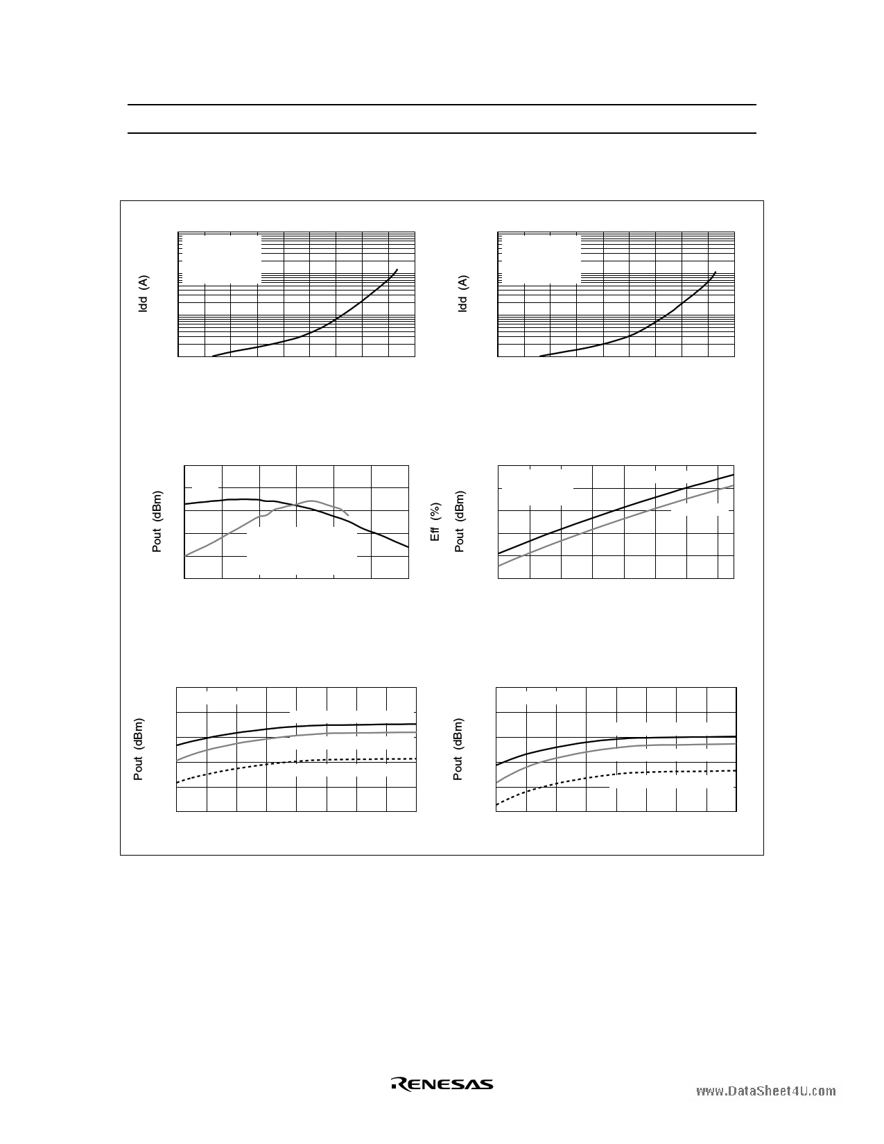
DCS mode (1710MHz to 1785 MHz) (cont)
DCS mode (1710 MHz) Idd vs. Pout
10
Pin = 0 dBm
Vdd = 3.5 V
Vapc = control
1 Tc = 25°C
www.DataSheet4U.com
0.1
0.01
–50 –40 –30 –20 –10 0 10 20 30 40
Pout (dBm)
PF08122B
DCS mode (1785 MHz) Idd vs. Pout
10
Pin = 0 dBm
Vdd = 3.5 V
Vapc = control
1 Tc = 25°C
0.1
0.01
–50 –40 –30 –20 –10 0 10 20 30 40
Pout (dBm)
DCS mode Pout, Eff vs. Freq
35 60
34 Pout
33
32
31
30
1600
Eff
Vdd = 3.5 V
Tc = 25°C
Pout:Vapc = 2.2 V
Eff:Pout = 32.5 dBm
1650 1700 1750 1800 1850
Freq (MHz)
55
50
45
40
35
1900
DCS mode Pout vs. Vdd
36.0
35.0
34.0
Pin = 0 dBm
Vapc = 2.2 V
Tc = 25°C
1710 MHz
1785 MHz
33.0
32.0
31.0
3
3.2 3.4 3.6 3.8 4
Vdd (V)
4.2 4.4
DCS mode (1710 MHz) Pout vs. Pin (Temperature variation)
35.0
Vapc = 2.2 V
34.0
Vdd = 3.5 V, Tc = 25°C
33.0
Vdd = 3.5 V, Tc = 85°C
32.0
31.0
Vdd = 3.1 V, Tc = 85°C
30.0
–8 –6 –4 –2 0 2 4 6 8
Pin (dBm)
DCS mode (1785 MHz) Pout vs. Pin (Temperature variation)
35.0
Vapc = 2.2 V
34.0
33.0
Vdd = 3.5 V, Tc = 25°C
32.0
Vdd = 3.5 V, Tc = 85°C
31.0
Vdd = 3.1 V, Tc = 85°C
30.0
–8 –6 –4 –2 0 2 4 6 8
Pin (dBm)
Rev.8, Jul. 2002, page 9 of 11
11 Page | ||
| Páginas | Total 13 Páginas | |
| PDF Descargar | [ Datasheet 08122B.PDF ] | |
Hoja de datos destacado
| Número de pieza | Descripción | Fabricantes |
| 08122B | PF08122B | RENESAS |
| Número de pieza | Descripción | Fabricantes |
| SLA6805M | High Voltage 3 phase Motor Driver IC. |
Sanken |
| SDC1742 | 12- and 14-Bit Hybrid Synchro / Resolver-to-Digital Converters. |
Analog Devices |
|
DataSheet.es es una pagina web que funciona como un repositorio de manuales o hoja de datos de muchos de los productos más populares, |
| DataSheet.es | 2020 | Privacy Policy | Contacto | Buscar |
