|
|
|
PDF IQX160 Data sheet ( Hoja de datos )
| Número de pieza | IQX160 | |
| Descripción | IQX Series | |
| Fabricantes | I-CUBE | |
| Logotipo | ||
Hay una vista previa y un enlace de descarga de IQX160 (archivo pdf) en la parte inferior de esta página. Total 65 Páginas | ||
|
No Preview Available !
et4U.com IQX Family Data SheetFEATURES
he• SRAM-based, in-system programmable
taS• Switch Matrix
a— Non-Blocking
.D— Identical and predictable delays
— One-to-one, one-to-many and many-to-one connections
ww• RapidConfigure™ parallel interface for fast, incremental
w configuration of Switch Matrix and I/O Port attributes
m— 100% JTAG compliant
• Clocked, Latched and Flow-through Dataflow Modes
o— As low as 7.5 ns pin-to-pin delay in flow-through mode
.cand 133 MHz clock rate in registered mode
• I/O Ports
— Individually programmable as input, output or
Ubidirectional
t4— For each I/O Port, clock, clock enable, input enable and
output enable can be selected independently from a large
epool of common control signals
— 12 mA current drive
e— Separated I/O power pins for easy interfacing between
h5V and 3.3V signals
DESCRIPTION
The IQX family of SRAM-based bit-oriented switching devices is
manufactured using a 0.6µ m CMOS process. These devices
offer clock speeds of up to 133 MHz and pin-to-pin delay as low
as 7.5 ns.
The IQX devices are used in applications requiring dynamic
switching and flexible routing / interconnection of signals. These
applications include communication switches, network systems,
DSP / image processing engines and file/video servers.
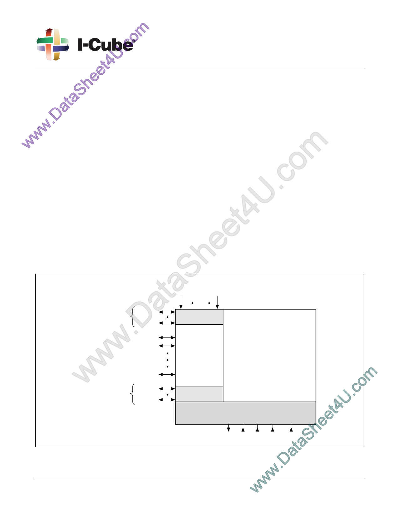
At the heart of IQX devices is a non-blocking Switch Matrix. A
line in the Switch Matrix can be connected to one or more other
lines. The Switch Matrix lines are connected to I/O Ports with
programmable functional attributes.
The RapidConfigure parallel interface allows connections in the
Switch Matrix to be changed quickly and incrementally. This
interface can also be used to configure I/O Port attributes
individually and incrementally. In either case, data integrity is
maintained on all unchanged signal paths through the device.
The IQX devices support the industry standard JTAG (IEEE
1149.1) interface for boundary scan testing. The same interface
can also used for serially downloading the configuration bit
stream into the devices.
taSShared with
aI/O Control
Signals
I/O Port
I/O Port
.DI/O Port
I/O Port
www omShared with
.cRapidConfigure
t4UInterface Signals
I/O Port
I/O Port
I/O Port
Dedicated
I/O Control Signals
I/O
Control
Signal
Ports
Switch Matrix
[Crossbar Array]
RapidConfigure
Interface
JTAG Configuration Control
heeTDO TDI TMS TCK TRST*
taSFigure 1. IQX Functional Block Diagram
www.DaJune 2000
Revision 5.0
1
1 page 
Figures
Figure 1. IQX Functional Block Diagram ..................................................................................................1
Figure 2. Switch Matrix Structure ..............................................................................................................9
Figure 3. Switch Matrix Control...............................................................................................................10
Figure 4. Programmable I/O Port .............................................................................................................10
Figure 5. IQX Output Driver and Pull-Up Current...................................................................................10
Figure 6. I/O Control ................................................................................................................................14
Figure 7. IQX RapidConfigure System Interface .....................................................................................16
Figure 8. Reset Circuit ..............................................................................................................................23
Figure 9. Off-line Bit Stream Generation .................................................................................................25
Figure 10. Embedded Bit Stream Generation ...........................................................................................25
Figure 11. Configuring Multiple IQX Devices.........................................................................................26
Figure 12. Test Circuit and Waveform Definition....................................................................................36
Figure 13. Registered Input and Registered Output Mode Timing (ICLK, OCLK Synchronized)..........36
Figure 14. Registered Input Mode Timing ...............................................................................................36
Figure 15. Registered Output Mode Timing.............................................................................................37
Figure 16. I/O Port Timing (Flow–through Mode)...................................................................................37
Figure 17. Input Enable Timing (Flow–through Mode) ...........................................................................37
Figure 18. Output Enable Timing (Flow–through Mode) ........................................................................38
Figure 19. Latched Input Mode Timing....................................................................................................38
Figure 20. Latched Output Mode Timing .................................................................................................38
Figure 21. Key Timing for Register Input, Clock Enable (CKE).............................................................39
Figure 22. Key Timing for Register Output, Clock Enable (CKE) ..........................................................39
Figure 23. Key Timing for Input Enable ..................................................................................................39
Figure 24. Key Timing for Output Enable................................................................................................40
Figure 25. Key Timing for Latch Input, Enable (CKE)............................................................................40
Figure 26. Key Timing for Latch Output, Enable (CKE) .........................................................................40
Figure 27. Key Counter Timing................................................................................................................41
Figure 28. RapidConfigure Timing ..........................................................................................................41
Figure 29. JTAG Timing ..........................................................................................................................42
Figure 30. IQX320 [PBGA/416L] Package Footprint..............................................................................45
Figure 31. IQX240B [PQFP/304L] Package Pinout ..................................................................................48
Figure 32. IQX160 [PQFP/208L] Package Pinout ...................................................................................51
Figure 33. IQX128B [PQFP/184L] Package Pinout.................................................................................54
Figure 34. IQX320 [PBGA/416L] Package Dimensions..........................................................................55
Figure 35. PQFP Package Dimensions .....................................................................................................56
June 2000
Revision 5.0
5
5 Page 
IQX Family Data Sheet
Symbol
Px Ax
0
Px 0
CLK
CKE
IE
IE
0
DQ
1
Ax
7
7
CE
Px
CLK
CKE
DQ
IE
LE
Ax
Ax Px
OE
Ax
CLK
CKE
DQ
LE
Px
OE
I/O Port Function
Input - The external signal is buffered from the I/O Port pin to the corresponding Switch Matrix
line. In this mode an optional input enable (IE) can be selected. Either polarity can be selected
for IE. The default level is a logic 1.
Mnemonic
IN
Registered Input (with variable length shift register and inversion) - The external signal at the
I/O Port pin is registered into a 7-bit edge-triggered shift register within the I/O Port. An 8-to-1
mux selects either the input (bit 0) or one of the 7 output bits of the shift register and connects
it to the corresponding signal line in the Switch Matrix through a register. Any tap on the shift
register can be selected. The true or complement of the incoming signal can be selected. The
default is bit 0, true value. A clock source is required in this mode. Either edge of CLK can be
selected. The default for CLK is rising edge. A clock enable (CKE) and input enable (IE) are
also available but not required. Either polarity can be selected for IE and CKE. The default
level for IE and CKE is a logic 1. The outputs of the shift register are unknown after hardware
reset (TRST* = 0).
RI&
[bit = value]&
[INV = value]
Latched Input - The external signal at the I/O Port pin is latched by a level-sensitive flip-flop
within the I/O Port. A latch enable source is required in this mode. The latch enable source is
composed of CLK and CKE, and at least one must be specified. An input enable (IE) is also
available but not required. Either polarity can be selected for CLK, CKE and IE. The default
level for all three is a logic 1. The output of the flip-flop is unknown after hardware reset
(TRST* = 0).
Output - The internal signal is buffered from the corresponding Switch Matrix line to the I/O
Port pin. In this mode an optional output enable (OE) can be selected. Either polarity can be
selected for OE. The default level is a logic 0.
LI
OP
Latched Output- The internal signal on the Switch Matrix line is latched by a level-sensitive
flip-flop within the I/O Port. A latch enable source is required in this mode. The latch enable
source is composed of CLK and CKE, and at least one must be specified. An output enable
(OE) is also available but not required. Either polarity can be selected for CLK and CKE. The
default level for both is a logic 1. Either polarity can be selected for OE. The default level is a
logic 0. The output of the flip-flop is unknown after hardware reset (TRST* = 0).
LO
Ax
CLK
CKE
DQ
Px
CE OE
IE
Px Ax
OE
Registered Output - The internal signal on the Switch Matrix line is registered by an edge-
triggered flip-flop within the I/O Port. A clock source is required in this mode. Either edge of
CLK can be selected. The default for CLK is rising edge. A clock enable (CKE) and output
enable (OE) are also available but not required. Either polarity can be selected for CKE and
OE. The default level for CKE is a logic 1 and the default level for OE is a logic 0. The output
of the flip-flop is unknown after hardware reset (TRST* = 0).
Bidirectional Transceiver - In this mode, the I/O buffer acts as a bidirectional transceiver
between the I/O Port pin and the corresponding Switch Matrix line. This mode requires an
input enable (IE) and output enable (OE). Either polarity can be selected for each but the
default level for IE is a logic 1 and the default level for OE is a logic 0. When the same source
(with default polarities) is used for IE and OE, it effectively acts as direction control. When the
same control signal (with one polarity inverted) is used for IE and OE, it effectively acts as a
Bus Repeater (BR) (see below) when both are enabled, and as No Connect (NC) when neither
is enabled.
RO
BT
Table 1. Summary of Programmable I/O Attributes for IQX Devices
June 2000
Revision 5.0
11
11 Page | ||
| Páginas | Total 65 Páginas | |
| PDF Descargar | [ Datasheet IQX160.PDF ] | |
Hoja de datos destacado
| Número de pieza | Descripción | Fabricantes |
| IQX160 | IQX Series | I-CUBE |
| Número de pieza | Descripción | Fabricantes |
| SLA6805M | High Voltage 3 phase Motor Driver IC. |
Sanken |
| SDC1742 | 12- and 14-Bit Hybrid Synchro / Resolver-to-Digital Converters. |
Analog Devices |
|
DataSheet.es es una pagina web que funciona como un repositorio de manuales o hoja de datos de muchos de los productos más populares, |
| DataSheet.es | 2020 | Privacy Policy | Contacto | Buscar |