|
|
|
PDF TA1322FN Data sheet ( Hoja de datos )
| Número de pieza | TA1322FN | |
| Descripción | DOWB-CONVERTER IC WITH PLL FOR SATELLITE TUNER | |
| Fabricantes | Toshiba Semiconductor | |
| Logotipo | ||
Hay una vista previa y un enlace de descarga de TA1322FN (archivo pdf) en la parte inferior de esta página. Total 21 Páginas | ||
|
No Preview Available !
Preliminary TOSHIBA Bipolar Linear Integrated Circuit Silicon Monolithic
TA1322FN
TA1322FN
Down-Converter IC with PLL for Satellite Tuner
The TA1322FN is a wideband down-converter which can
operate at input frequency ranging from 850 MHz to 2200 MHz.
Intended primarily for use in satellite tuners, this IC includes an
oscillator, a mixer, an IF amplifier and a PLL.
The I2C bus data format is used as the data control format.
The supply voltage of 5.0 V helps minimize the tuner’s power
dissipation, while the compact 30-pin SSOP package allows the
tuner to be kept small.
Features
· Supply voltage: 5.0 V (typ.)
· Wide input frequency range
· Low phase noise oscillator
Weight: 0.17 g (typ.)
· Standard I2C bus format control
· 4-MHz (X’tal) buffer output pin
· Reference oscillator input change-over switch [X’tal or external input]
· 33-V high-voltage tuning amplifier built-in
· Built-in comparator (P4, P5, P7)
· Bandswitch drive transistor (P0) [IBD = 40 mA (max)]
· Selected IF output port
· Frequency step: 62.5 kHz or 125 kHz (for 4-MHz X’tal)
· 4-address setting via address selector
· Power-on reset circuit
· ×1/2 prescaler
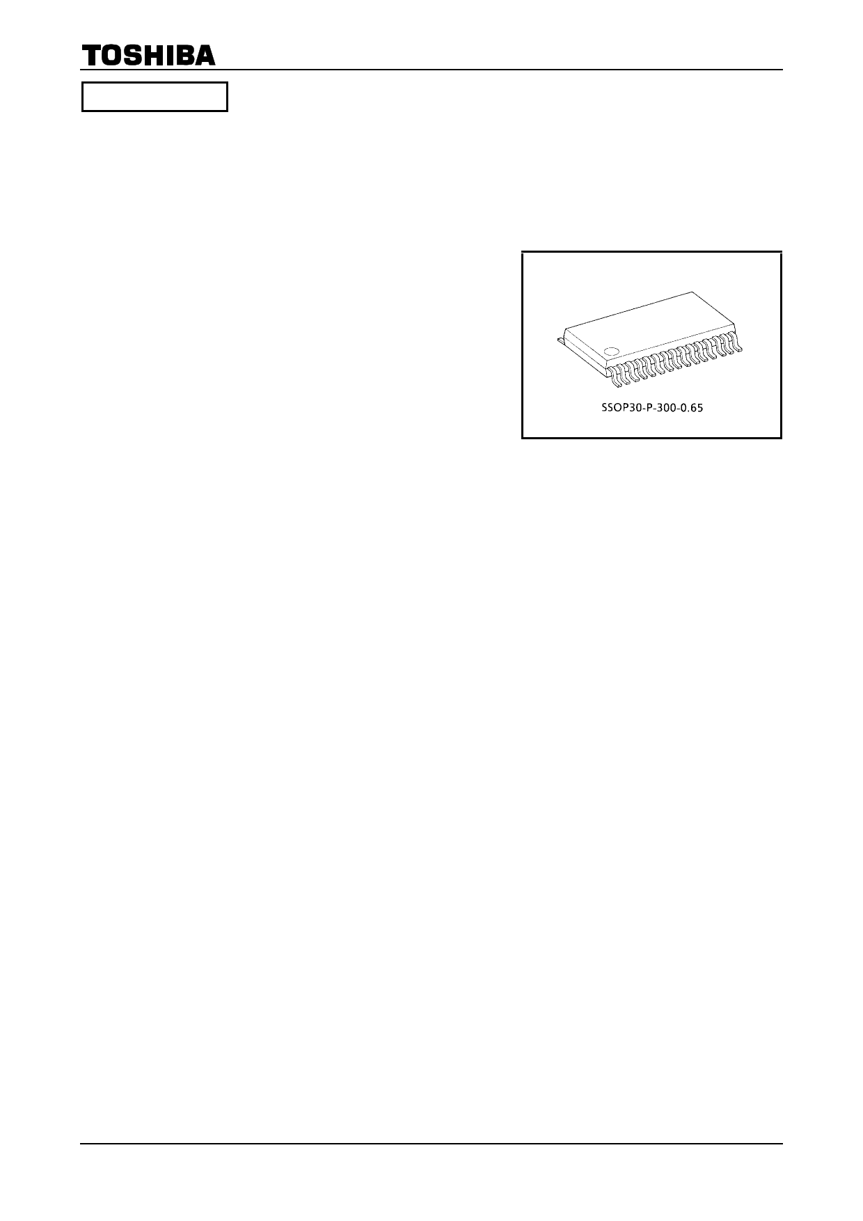
· Flat compact package: SSOP30-P-300-0.65 (0.65-mm pitch)
Power-On Reset Operation Conditions
· Frequency step: 125 kHz
· Charge pump output current: ±50 µA
· Counter data: all [0]
· Band driver: OFF
· Tuning amplifier: OFF
· IF output operation: pin 19 is ON
Note 1: This device can easily be damaged by high voltages or electrical fields. For this reason, please handle it
with care.
1 2002-02-12
1 page 
Pin No.
Pin Name
19 IF Output 1
21 IF Output 2
20 GND4
22 VCC3
23 GND5
Function
IF output pin.
Output can be controlled by setting
the band switch data (P6).
IF output impedance is 75 W each
other.
When P6 data set 0, output pin is Pin
19 (IF output 1).
When P6 data set 1, output pin is Pin
21 (IF output 2).
Ground pin for IF amplifier circuit
block
Power supply pin for IF amplifier
circuit block
Ground pin for IF amplifier circuit
block
24 XO Switch
Determines reference signal input.
If connected to ground:
X’tal oscillator.
If open or connected to VCC2:
external input
25 TEST
When test mode set, this pin can
confirm X’tal divider signal and 1/2
counter signal.
This pin can be used at open.
26 GND6
27 RF Input1
28 RF Input2
29 GND7
30 VCC4
Ground pin for mixer circuit block
RF signal input pin
Input can be either balanced or
unbalanced.
Ground pin for mixer circuit block
Power supply pin for mixer circuit
block
TA1322FN
Interface
VCC3
19, 21
VCC2
GND4, 5
¾
¾
¾
1 kW
24
GND3
VCC2
25
GND3
¾
27
3 kW
GND7
¾
¾
28
5 2002-02-12
5 Page 
TA1322FN
PLL Block
--I2C Bus Communications Control--
The TA1322FN conforms to Standard Mode I2C bus format.
I2C Bus Mode allows two-way bus communication using Write Mode (for receiving data) and Read Mode (for
processing status data).
Write Mode or Read Mode can be selected by setting the least significant bit (R/W bit) of the address byte.
If the least significant address bit is set to 0, Write Mode is selected; if it is set to 1, Read Mode is selected.
Address can be set using the hardware bits. 4 programmable address can be programmed.
Using this setting, multiple frequency synthesizers can be used on the same I2C bus line.
The address for the hardware bit setting can be selected by applying voltage to the address setting pin (ADR-pin
18). The address is selected according to the setting of these bits.
During acknowledgment of receipt of a valid address byte, the serial data (SDA) line is Low.
If Write Mode is currently selected, when the data byte is programmed, the serial data (SDA) line will be Low
during the next acknowledgment.
A) Write mode (setting command)
When Write Mode is selected, byte 1 holds address data; byte 2 and byte 3 hold frequency data; byte
4 holds the divider ratio setting and function setting data; and byte 5 holds output port data.
Data is latched and transferred at the end of byte 3, byte 4 and byte 5.
Byte 2 and byte 3 are latched and transferred as a byte pair.
Once a valid address has been received and acknowledged, the data type can be determined by
reading the first bit of the next byte. That is, if the first bit is 0, the data is frequency data; if it is 1,
the data is function-setting or band output data.
Additional data can be input without the need to transmit the address data again until the I2C bus
STOP condition is detected (e.g. a frequency sweep using additional frequency data is possible).
If a data transmission is aborted, data programmed before the abort remains valid.
[[BYTE 1]]
The address data for byte 1 can be set using the hardware bit.
The hardware bit can be set by applying a voltage to the address-setting pin (ADR: pin 18).
[[BYTE 2, BYTE 3]]
Byte 2, byte 3 control the 15-bit programmable counter ratio and are stored in the 15-bit shift
register together with frequency setting counter data.
The program frequency can be calculated using the following formula:
fosc = 2 ´ fr ´ N
fosc: Program frequency
fr: Phase comparator reference frequency
N: Counter total divider ratio
fr is calculated from the crystal oscillator frequency and the reference frequency divider ratio
set in byte 4 (the control byte).
(fr = X’tal oscillator frequency/reference divider ratio)
The reference frequency divider ratio can be set to 1/64 or 1/128.
When a 4-MHz crystal oscillator is used, fr = 62.5 kHz or 31.25 kHz. The respective step
frequencies are 125 kHz and 62.5 kHz.
[[BYTE 4]]
Byte 4 is a control byte used to set function. Bit 2 (CP) controls the output current of the
charge-pump circuit.
When bit 2 is set to [0], the output current is set to ±50 mA; when set to [1], ±240 mA.
Bit 3 (T1) is used to set the test mode. When bit 3 is set to [0], normal mode; when set to [1],
test mode.
Bit 4 (T0) is used to set the charge pump. When bit 4 is set to [0], charge pump is ON (normal
used); When set to [1], charge pump is OFF.
Bit 5 (TS2) and bit 6 (TS1) used to set the test mode. They are used to set the charge pump test,
phase comparator reference signal output, and 1/2 counter divider ratios.
Bit 7 (TS0) is used to set the X’tal reference frequency divider ratio. When bit 7 is set to [0],
1/128 (frequency step is 62.5 kHz); when set to [1], 1/64 (frequency step is 125 kHz).
Bit 8 (OS) is used to set the charge pump drive amplifier output setting. When bit 8 is set to [0],
11 2002-02-12
11 Page | ||
| Páginas | Total 21 Páginas | |
| PDF Descargar | [ Datasheet TA1322FN.PDF ] | |
Hoja de datos destacado
| Número de pieza | Descripción | Fabricantes |
| TA1322FN | DOWB-CONVERTER IC WITH PLL FOR SATELLITE TUNER | Toshiba Semiconductor |
| Número de pieza | Descripción | Fabricantes |
| SLA6805M | High Voltage 3 phase Motor Driver IC. |
Sanken |
| SDC1742 | 12- and 14-Bit Hybrid Synchro / Resolver-to-Digital Converters. |
Analog Devices |
|
DataSheet.es es una pagina web que funciona como un repositorio de manuales o hoja de datos de muchos de los productos más populares, |
| DataSheet.es | 2020 | Privacy Policy | Contacto | Buscar |