|
|
|
PDF AD9515 Data sheet ( Hoja de datos )
| Número de pieza | AD9515 | |
| Descripción | 1.6 GHz Clock Distribution IC | |
| Fabricantes | Analog Devices | |
| Logotipo | ||
Hay una vista previa y un enlace de descarga de AD9515 (archivo pdf) en la parte inferior de esta página. Total 29 Páginas | ||
|
No Preview Available !
Data Sheet
1.6 GHz Clock Distribution IC, Dividers,
Delay Adjust, Two Outputs
AD9515
FEATURES
1.6 GHz differential clock input
2 programmable dividers
Divide-by in range from1 to 32
Phase select for coarse delay adjust
1.6 GHz LVPECL clock output
Additive output jitter 225 fs rms
800 MHz/250 MHz LVDS/CMOS clock output
Additive output jitter 300 fs rms/290 fs rms
Time delays up to 10 ns
Device configured with 4-level logic pins
Space-saving, 32-lead LFCSP
APPLICATIONS
Low jitter, low phase noise clock distribution
Clocking high speed ADCs, DACs, DDSs, DDCs, DUCs, MxFEs
High performance wireless transceivers
High performance instrumentation
Broadband infrastructure
ATE
GENERAL DESCRIPTION
The AD9515 features a two-output clock distribution IC in a
design that emphasizes low jitter and phase noise to maximize
data converter performance. Other applications with
demanding phase noise and jitter requirements also benefit
from this part.
There are two independent clock outputs. One output is
LVPECL, while the other output can be set to either LVDS or
CMOS levels. The LVPECL output operates to 1.6 GHz. The
other output operates to 800 MHz in LVDS mode and to
250 MHz in CMOS mode.
Each output has a programmable divider that can be set to
divide by a selected set of integers ranging from 1 to 32. The
phase of one clock output relative to the other clock output can
be set by means of a divider phase select function that serves as
a coarse timing adjustment.
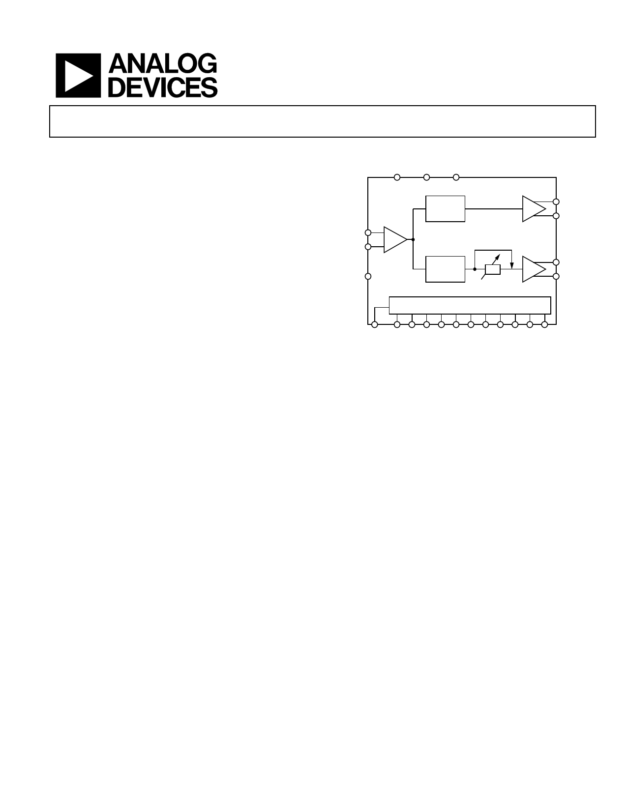
CLK
CLKB
SYNCB
FUNCTIONAL BLOCK DIAGRAM
RSET
VS
GND
AD9515 LVPECL
/1. . . /32
OUT0
OUT0B
/1. . . /32
LVDS/CMOS
OUT1
∆t
OUT1B
SETUP LOGIC
VREF S10 S9 S8 S7 S6 S5 S4 S3 S2 S1 S0
Figure 1.
The LVDS/CMOS output features a delay element with three
selectable full-scale delay values (1.5 ns, 5 ns, and 10 ns), each
with 16 steps of fine adjustment.
The AD9515 does not require an external controller for
operation or setup. The device is programmed by means of
11 pins (S0 to S10) using 4-level logic. The programming pins
are internally biased to ⅓ VS. The VREF pin provides a level of
⅔ VS. VS (3.3 V) and GND (0 V) provide the other two logic levels.
The AD9515 is ideally suited for data converter clocking
applications where maximum converter performance is
achieved by encode signals with subpicosecond jitter.
The AD9515 is available in a 32-lead LFCSP and operates from
a single 3.3 V supply. The temperature range is −40°C to +85°C.
Rev. A
Information furnished by Analog Devices is believed to be accurate and reliable. However, no
responsibilityisassumedbyAnalogDevices for itsuse,nor foranyinfringementsofpatentsor other
rights of third parties that may result from its use. Specifications subject to change without notice. No
license is granted by implication or otherwise under any patent or patent rights of Analog Devices.
Trademarksandregisteredtrademarksarethepropertyoftheirrespectiveowners.
One Technology Way, P.O. Box 9106, Norwood, MA 02062-9106, U.S.A.
Tel: 781.329.4700
www.analog.com
Fax: 781.461.3113 © 2005–2012 Analog Devices, Inc. All rights reserved.
1 page 
AD9515
TIMING CHARACTERISTICS
CLK input slew rate = 1 V/ns or greater.
Table 3.
Parameter
LVPECL
Output Rise Time, tRP
Output Fall Time, tFP
PROPAGATION DELAY, tPECL, CLK-TO-LVPECL OUT
Divide = 1
Divide = 2 − 32
Variation with Temperature
OUTPUT SKEW, LVPECL OUTPUT
LVPECL
OUT
Across
Multiple
Parts,
t1
SKP_AB3
LVDS
Output Rise Time, tRL
Output Fall Time, tFL
PROPAGATION DELAY, tLVDS, CLK-TO-LVDS OUT
OUT3 to OUT4
Divide = 1
Divide = 2 − 32
Variation with Temperature
OUTPUT SKEW, LVDS OUTPUT
LVDS
OUT
Across
Multiple
Parts,
t1
SKV_AB
CMOS
Output Rise Time, tRC
Output Fall Time, tFC
PROPAGATION DELAY, tCMOS, CLK-TO-CMOS OUT
Divide = 1
Divide = 2 − 32
Variation with Temperature
OUTPUT SKEW, CMOS OUTPUT
CMOS
OUT
Across
Multiple
Parts,
t1
SKC_AB
LVPECL-TO-LVDS OUT
Output Delay, tSKP_V
LVPECL-TO-CMOS OUT
Output Delay, tSKP_C
DELAY ADJUST (OUT2; LVDS AND CMOS)
S0 = 1/3
Zero Scale Delay Time2
Zero Scale Variation with Temperature
Full Scale Time Delay2
Full Scale Variation with Temperature
S0 = 2/3
Zero Scale Delay Time2
Zero Scale Variation with Temperature
Full Scale Time Delay2
Full Scale Variation with Temperature
Data Sheet
Min Typ
60
60
355 480
395 530
0.5
200
210
1.00 1.25
1.05 1.30
0.9
650
650
1.10 1.45
1.15 1.50
1
700 970
0.88 1.14
Max Unit Test Conditions/Comments
100 ps
Termination = 50 Ω to VS − 2 V
20% to 80%, measured differentially
100 ps
80% to 20%, measured differentially
635 ps
710 ps
ps/°C
125 ps
350 ps
350 ps
Termination = 100 Ω differential
20% to 80%, measured differentially
80% to 20%, measured differentially
Delay off on OUT4
1.55
1.60
230
865
990
1.75
1.80
300
1150
1.43
ns
ns
ps/°C
ps
ps
ps
ns
ns
ps/°C
ps
ps
ns
Delay off on OUT4
B outputs are inverted; termination = open
20% to 80%; CLOAD = 3 pF
80% to 20%; CLOAD = 3 pF
Delay off on OUT4
Delay off on OUT4
Everything the same; different logic type
LVPECL to LVDS on same part
Everything the same; different logic type
LVPECL to CMOS on same part
0.34
0.20
1.7
−0.38
0.45
0.31
5.9
−1.3
ns
ps/°C
ns
ps/°C
ns
ps/°C
ns
ps/°C
Rev. A | Page 4 of 28
5 Page 
AD9515
Data Sheet
POWER
Table 7.
Parameter
POWER-ON SYNCHRONIZATION1
VS Transit Time from 2.2 V to 3.1 V
POWER DISSIPATION
POWER DELTA
Divider (Divide = 2 to Divide = 1)
LVPECL Output
LVDS Output
CMOS Output (Static)
CMOS Output (@ 62.5 MHz)
CMOS Output (@ 125 MHz)
Delay Block
Min Typ Max Unit Test Conditions/Comments
35 ms See the Power-On SYNC section.
215 285 380 mW Both outputs on. LVPECL (divide = 2), LVDS (divide = 2). No clock.
Does not include power dissipated in external resistors.
300 370 465 mW Both outputs on. LVPECL (divide = 2), CMOS (divide = 2);
at 62.5 MHz out (5 pF load).
330 405 510 mW Both outputs on. LVPECL, CMOS (divide = 2);
at 125 MHz out (5 pF load).
15 30 45 mW For each divider. No clock.
65 90 125 mW For each output. No clock.
20 50 85 mW No clock.
30 40 50 mW No clock.
80 110 140 mW Single-ended. At 62.5 MHz out with 5 pF load.
110 150 190 mW Single-ended. At 125 MHz out with 5 pF load.
30 45 65 mW Off to 1.5 ns fs, delay word = 60; output clocking at 62.5 MHz.
1 This is the rise time of the VS supply that is required to ensure that a synchronization of the outputs occurs on power-up. The critical factor is the time it takes the VS to
transition the range from 2.2 V to 3 .1 V. If the rise time is too slow, the outputs will not be synchronized.
Rev. A | Page 10 of 28
11 Page | ||
| Páginas | Total 29 Páginas | |
| PDF Descargar | [ Datasheet AD9515.PDF ] | |
Hoja de datos destacado
| Número de pieza | Descripción | Fabricantes |
| AD9510 | 1.2 GHz Clock Distribution IC | Analog Devices |
| AD9511 | 1.2 GHz Clock Distribution IC | Analog Devices |
| AD9512 | 1.2 GHz Clock Distribution IC | Analog Devices |
| AD9513 | 800 MHz Clock Distribution IC | Analog Devices |
| Número de pieza | Descripción | Fabricantes |
| SLA6805M | High Voltage 3 phase Motor Driver IC. |
Sanken |
| SDC1742 | 12- and 14-Bit Hybrid Synchro / Resolver-to-Digital Converters. |
Analog Devices |
|
DataSheet.es es una pagina web que funciona como un repositorio de manuales o hoja de datos de muchos de los productos más populares, |
| DataSheet.es | 2020 | Privacy Policy | Contacto | Buscar |