|
|
|
PDF LM4917SD Data sheet ( Hoja de datos )
| Número de pieza | LM4917SD | |
| Descripción | Ground-Referenced/ 95mW Stereo Headphone Amplifier | |
| Fabricantes | National Semiconductor | |
| Logotipo | ||
Hay una vista previa y un enlace de descarga de LM4917SD (archivo pdf) en la parte inferior de esta página. Total 18 Páginas | ||
|
No Preview Available !
November 2004
LM4917
Ground-Referenced, 95mW Stereo Headphone Amplifier
General Description
The LM4917 is a stereo, output capacitor-less headphone
amplifier capable of delivering 95mW of continuous average
power into a 16Ω load with less than 1% THD+N from a
single 3V power supply.
The LM4917 provides high quality audio reproduction with
minimal external components. A ground referenced output
eliminates the output coupling capacitors typically required
by single-ended loads, reducing component count, cost and
board space consumption. This makes the LM4917 ideal for
mobile phones and other portable equipment where board
space is at a premium. Eliminating the output coupling ca-
pacitors also improves low frequency response.
The LM4917 operates from a single 1.4V to 3.6V power
supply, features low 0.02% THD+N and 70dB PSRR. Inde-
pendent right/left channel low-power shutdown controls pro-
vide power saving flexibility for mono/stereo applications.
Superior click and pop suppression eliminates audible tran-
sients during start up and shutdown. Short circuit and ther-
mal overload protection protects the device during fault con-
ditions.
Key Specifications
j Improved PSRR at 1kHz
j Power Output at VDD = 3V,
RL = 16Ω, THD % 1%
j Shutdown Current
70dB (typ)
95mW (typ)
0.01µA (typ)
Features
n Ground referenced outputs
n High PSRR
n Available in space-saving TSSOP package
n Ultra low current shutdown mode
n Improved pop & click circuitry eliminates noises during
turn-on and turn-off transitions
n 1.4 – 3.6V operation
n No output coupling capacitors, snubber networks,
bootstrap capacitors
n Shutdown either channel independently
Applications
n Notebook PCs
n Desktop PCs
n Mobile Phone
n PDAs
n Portable electronic devices
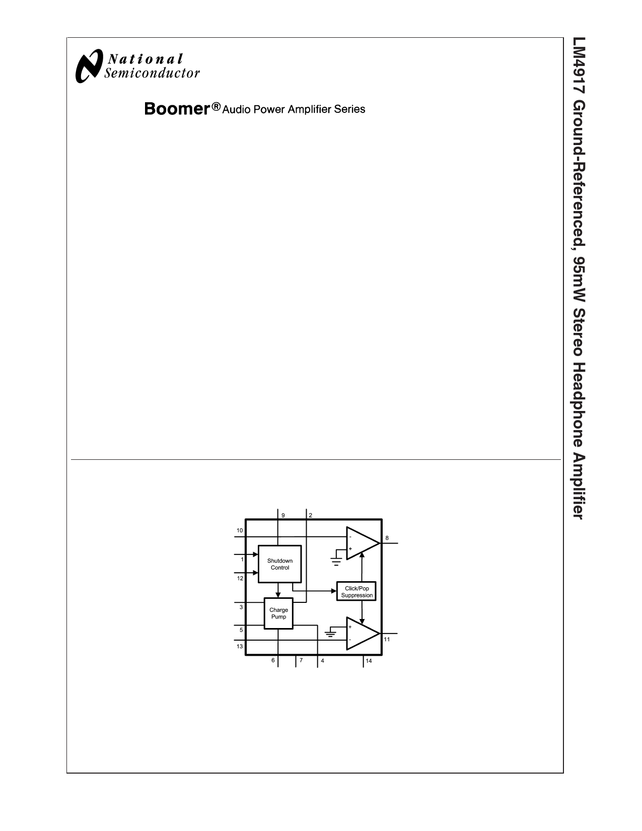
Block Diagram
200893B8
FIGURE 1. Circuit Block Diagram
Boomer® is a registered trademark of National Semiconductor Corporation.
© 2004 National Semiconductor Corporation DS200893
www.national.com
1 page 
External Components Description (Figure 1)
Components
1. Ri
2. Ci
3. Rf
4. C1
5. C2
6. C3
7. C4
Functional Description
Inverting input resistance which sets the closed-loop gain in conjunction with Rf. This resistor also forms a
high-pass filter with Ci at fc = 1 / (2πRiCi).
Input coupling capacitor which blocks the DC voltage at the amplifier’s input terminals. Also creates a
high-pass filter with Ri at fc = 1 / (2πRiCi). Refer to the section Proper Selection of External Components,
for an explanation of how to determine the value of Ci.
Feedback resistance which sets the closed-loop gain in conjunction with Ri.
Flying capacitor. Low ESR ceramic capacitor (≤100mΩ)
Output capacitor. Low ESR ceramic capacitor (≤100mΩ)
Tantalum capacitor. Supply bypass capacitor which provides power supply filtering. Refer to the Power Supply
Bypassing section for information concerning proper placement and selection of the supply bypass capacitor.
Ceramic capacitor. Supply bypass capacitor which provides power supply filtering. Refer to the Power Supply
Bypassing section for information concerning proper placement and selection of the supply bypass capacitor.
5 www.national.com
5 Page 
Application Information
ELIMINATING THE OUTPUT COUPLING CAPACITOR
The LM4917 features a low noise inverting charge pump that
generates an internal negative supply voltage. This allows
the outputs of the LM4917 to be biased about GND instead
of a nominal DC voltage, like traditional headphone amplifi-
ers. Because there is no DC component, the large DC
blocking capacitors (typically 220µF) are not necessary. The
coupling capacitors are replaced by two, small ceramic
charge pump capacitors, saving board space and cost.
Eliminating the output coupling capacitors also improves low
frequency response. The headphone impedance and the
output capacitor form a high pass filter that not only blocks
the DC component of the output, but also attenuates low
frequencies, impacting the bass response. Because the
LM4917 does not require the output coupling capacitors, the
low frequency response of the device is not degraded by
external components.
In addition to eliminating the output coupling capacitors, the
ground referenced output nearly doubles the available dy-
namic range of the LM4917 when compared to a traditional
headphone amplifier operating from the same supply volt-
age.
OUTPUT TRANSIENT (’CLICK AND POPS’)
ELIMINATED
The LM4917 contains advanced circuitry that virtually elimi-
nates output transients (’clicks and pops’). This circuitry
prevents all traces of transients when the supply voltage is
first applied or when the part resumes operation after coming
out of shutdown mode.
To ensure optimal click and pop performance under low gain
configurations (less than 0dB), it is critical to minimize the
RC combination of the feedback resistor RF and stray input
capacitance at the amplifier inputs. A more reliable way to
lower gain or reduce power delivered to the load is to place
a current limiting resistor in series with the load as explained
in the Minimizing Output Noise / Reducing Output Power
section.
AMPLIFIER CONFIGURATION EXPLANATION
As shown in Figure 2, the LM4917 has two operational
amplifiers internally. The two amplifiers have externally con-
figurable gain, and the closed loop gain is set by selecting
the ratio of Rf to Ri. Consequently, the gain for each channel
of the IC is
AV = -(Rf / Ri)
Since this an output ground-referenced amplifier, by driving
the headphone through ROUT (Pin 11) and LOUT (Pin 8), the
LM4917 does not require output coupling capacitors. The
typical single-ended amplifier configuration where one side
of the load is connected to ground requires large, expensive
output capacitors.
POWER DISSIPATION
Power dissipation is a major concern when using any power
amplifier and must be thoroughly understood to ensure a
successful design. Equation 1 states the maximum power
dissipation point for a single-ended amplifier operating at a
given supply voltage and driving a specified output load.
PDMAX = (VDD) 2 / (2π2RL)
(1)
Since the LM4917 has two operational amplifiers in one
package, the maximum internal power dissipation point is
twice that of the number which results from Equation 1. Even
with the large internal power dissipation, the LM4917 does
not require heat sinking over a large range of ambient tem-
perature. From Equation 1, assuming a 3V power supply and
a 16Ω load, the maximum power dissipation point is 28mW
per amplifier. Thus the maximum package dissipation point
is 56mW. The maximum power dissipation point obtained
must not be greater than the power dissipation that results
from Equation 2:
PDMAX = (TJMAX - TA) / (θJA)
(2)
For package TSSOP, θJA = 109˚C/W. TJMAX = 150˚C for the
LM4917. Depending on the ambient temperature, TA, of the
system surroundings, Equation 2 can be used to find the
maximum internal power dissipation supported by the IC
packaging. If the result of Equation 1 is greater than that of
Equation 2, then either the supply voltage must be de-
creased, the load impedance increased or TA reduced. For
the typical application of a 3V power supply, with a 16Ω load,
the maximum ambient temperature possible without violating
the maximum junction temperature is approximately 119.9˚C
provided that device operation is around the maximum
power dissipation point. Power dissipation is a function of
output power and thus, if typical operation is not around the
maximum power dissipation point, the ambient temperature
may be increased accordingly. Refer to the Typical Perfor-
mance Characteristics curves for power dissipation infor-
mation for lower output powers.
POWER SUPPLY BYPASSING
As with any power amplifier, proper supply bypassing is
critical for low noise performance and high power supply
rejection. Applications that employ a 3V power supply typi-
cally use a 4.7µF in parallel with a 0.1µF ceramic filter
capacitors to stabilize the power supply’s output, reduce
noise on the supply line, and improve the supply’s transient
response. However, their presence does not eliminate the
need for a local 0.1µF supply bypass capacitor, CS, con-
nected between the LM4917’s supply pins and ground. Keep
the length of leads and traces that connect capacitors be-
tween the LM4917’s power supply pin and ground as short
as possible.
MICRO POWER SHUTDOWN
The voltage applied to the SD_LC (shutdown left channel)
pin and the SD_RC (shutdown right channel) pin controls the
LM4917’s shutdown function. When active, the LM4917’s
micropower shutdown feature turns off the amplifiers’ bias
circuitry, reducing the supply current. The trigger point is
0.3*CPVDD for a logic-low level, and 0.7*CPVDD for logic-
high level. The low 0.01µA(typ) shutdown current is achieved
by appling a voltage that is as near as ground a possible to
the SD_LC/SD_RC pins. A voltage that is higher than ground
may increase the shutdown current.
There are a few ways to control the micro-power shutdown.
These include using a single-pole, single-throw switch, a
microprocessor, or a microcontroller. When using a switch,
connect an external 100kΩ pull-up resistor between the
SD_LC/SD_RC pins and VDD. Connect the switch between
the SD_LC/SD_RC pins and ground. Select normal amplifier
11 www.national.com
11 Page | ||
| Páginas | Total 18 Páginas | |
| PDF Descargar | [ Datasheet LM4917SD.PDF ] | |
Hoja de datos destacado
| Número de pieza | Descripción | Fabricantes |
| LM4917SD | Ground-Referenced/ 95mW Stereo Headphone Amplifier | National Semiconductor |
| Número de pieza | Descripción | Fabricantes |
| SLA6805M | High Voltage 3 phase Motor Driver IC. |
Sanken |
| SDC1742 | 12- and 14-Bit Hybrid Synchro / Resolver-to-Digital Converters. |
Analog Devices |
|
DataSheet.es es una pagina web que funciona como un repositorio de manuales o hoja de datos de muchos de los productos más populares, |
| DataSheet.es | 2020 | Privacy Policy | Contacto | Buscar |