|
|
|
PDF LM5008 Data sheet ( Hoja de datos )
| Número de pieza | LM5008 | |
| Descripción | High Voltage (100V) Step Down Switching Regulator | |
| Fabricantes | National Semiconductor | |
| Logotipo | ||
Hay una vista previa y un enlace de descarga de LM5008 (archivo pdf) en la parte inferior de esta página. Total 15 Páginas | ||
|
No Preview Available !
October 2004
LM5008
High Voltage (100V) Step Down Switching Regulator
General Description
The LM5008 Step Down Switching Regulator features all of
the functions needed to implement a low cost, efficient, Buck
bias regulator. This high voltage regulator contains an 100 V
N-Channel Buck Switch. The device is easy to implement
and is provided in the MSOP-8 and the thermally enhanced
LLP-8 packages. The regulator is based on a hysteretic
control scheme using an ON time inversely proportional to
VIN. This feature allows the operating frequency to remain
relatively constant. The hysteretic control requires no loop
compensation. An intelligent current limit is implemented
with forced OFF time, which is inversely proportional to Vout.
This scheme ensures short circuit protection while providing
minimum foldback. Other protection features include: Ther-
mal Shutdown, VCC under-voltage lockout, Gate drive under-
voltage lockout, and Max Duty Cycle limiter
Features
n Integrated 100V, N-Channel buck switch
n Internal VCC regulator
n No loop compensation required
n Ultra-Fast transient response
n On time varies inversely with line voltage
n Operating frequency remains constant with varying line
voltage and load current
n Adjustable output voltage
n Highly efficient operation
n Precision internal reference
n Low bias current
n Intelligent current limit protection
n Thermal shutdown
Typical Applications
n Non-Isolated Telecommunication Buck Regulator
n Secondary High Voltage Post Regulator
n +42V Automotive Systems
Package
n MSOP - 8
n LLP - 8 (4mm x 4mm)
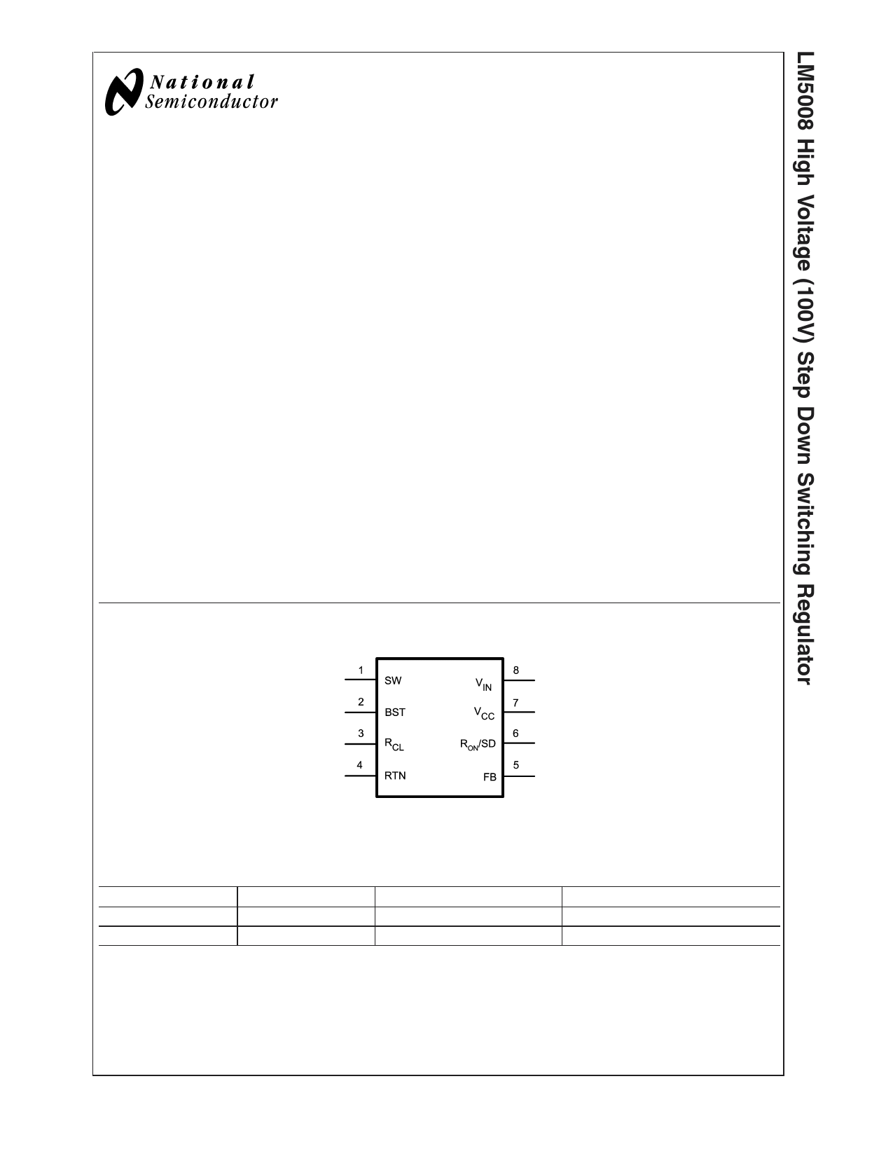
Connection Diagram
Ordering Information
Order Number
LM5008MM
LM5008SD
Package Type
MSOP-8
LLP-8
20097902
8-Lead MSOP, LLP
NSC Package Drawing
MUA08A
SDC08A
Supplied As
1000 Units on Tape and Reel
1000 Units on Tape and Reel
© 2004 National Semiconductor Corporation DS200979
www.national.com
1 page 
Electrical Characteristics (Continued)
Specifications with standard typeface are for TJ = 25˚C, and those with boldface type apply over full Operating Junction
Temperature range. VIN = 48V, unless otherwise stated (Note 3).
Symbol
Parameter
Conditions
Min Typ
Max
Units
Minimum Off Time
Minimum Off Timer
FB = 0V
300 ns
Regulation and OV Comparators
FB Reference Threshold
Internal reference
2.445
2.5
2.550
V
Trip point for switch ON
FB Over-Voltage Threshold
Trip point for switch OFF
2.875
V
FB Bias Current
100 nA
Thermal Shutdown
Tsd Thermal Shutdown Temp.
165 ˚C
Thermal Shutdown Hysteresis
25 ˚C
Thermal Resistance
θJA Junction to Ambient
MUA Package
SDC Package
200 ˚C/W
40 ˚C/W
Note 1: Absolute Maximum Ratings are limits beyond which damage to the device may occur. Operating Ratings are conditions under which operation of the device
is intended to be functional. For guaranteed specifications and test conditions, see the Electrical Characteristics.
Note 2: For detailed information on soldering plastic MSOP and LLP packages, refer to the Packaging Data Book available from National Semiconductor
Corporation.
Note 3: All limits are guaranteed. All electrical characteristics having room temperature limits are tested during production with TA = TJ = 25˚C. All hot and cold limits
are guaranteed by correlating the electrical characteristics to process and temperature variations and applying statistical process control.
Note 4: The VCC output is intended as a self bias for the internal gate drive power and control circuits. Device thermal limitations limit external loading.
Note 5: The human body model is a 100pF capacitor discharged through a 1.5kΩ resistor into each pin.
Note 6: For devices procured in the LLP-8 package the Rds(on) limits are guaranteed by design characterization data only.
5 www.national.com
5 Page 
Applications Information (Continued)
false triggering of the VCC UVLO at the buck switch on/off
transitions. For this reason, C3 should be no smaller than 0.1
µF.
C2, and R3: When selecting the output filter capacitor C2,
the items to consider are ripple voltage due to its ESR, ripple
voltage due to its capacitance, and the nature of the load.
a) ESR and R3: A low ESR for C2 is generally desirable so
as to minimize power losses and heating within the capaci-
tor. However, a hysteretic regulator requires a minimum
amount of ripple voltage at the feedback input for proper loop
operation. For the LM5008 the minimum ripple required at
pin 5 is 25 mV p-p, requiring a minimum ripple at VOUT1 of
100 mV. Since the minimum ripple current (at minimum Vin)
is 34 mA p-p, the minimum ESR required at VOUT1 is 100mV/
34mA = 2.94Ω. Since quality capacitors for SMPS applica-
tions have an ESR considerably less than this, R3 is inserted
as shown in Figure 1. R3’s value, along with C2’s ESR, must
result in at least 25 mV p-p ripple at pin 5. Generally, R3 will
be 0.5 to 3.0Ω.
b) Nature of the Load: The load can be connected to VOUT1
or VOUT2. VOUT1 provides good regulation, but with a ripple
voltage which ranges from 100 mV (@ Vin = 12V) to 500mV
(@Vin = 95V). Alternatively, VOUT2 provides low ripple, but
lower regulation due to R3.
For a maximum allowed ripple voltage of 100 mVp-p at
VOUT2 (@ Vin = 95V), assume an ESR of 0.4Ω for C2. At
maximum Vin, the ripple current is 181 mAp-p, creating a
ripple voltage of 72 mVp-p. This leaves 28 mVp-p of ripple
due to the capacitance. The average current into C2 due to
the ripple current is calculated using the waveform in Figure
12.
FIGURE 12. Inductor Current Waveform
20097926
Starting when the current reaches Io (300 mA in Figure 12)
half way through the on-time, the current continues to in-
crease to the peak (391 mA), and then decreases to 300 mA
half way through the off-time. The average value of this
portion of the waveform is 45.5mA, and will cause half of the
voltage ripple, or 14 mV. The interval is one half of the
frequency cycle time, or 2.23 µs. Using the capacitor’s basic
equation:
C = I x ∆t / ∆V
the minimum value for C2 is 7.2 µF. The ripple due to C2’s
capacitance is 90˚ out of phase from the ESR ripple, and the
two numbers do not add directly. However, this calculation
provides a practical minimum value for C2 based on its ESR,
and the target spec. To allow for the capacitor’s tolerance,
temperature effects, and voltage effects, a 15 µF, X7R ca-
pacitor will be used.
c) In summary: The above calculations provide a minimum
value for C2, and a calculation for R3. The ESR is just as
important as the capacitance. The calculated values are
guidelines, and should be treated as starting points. For
each application, experimentation is needed to determine
the optimum values for R3 and C2.
RCL: When a current limit condition is detected, the minimum
off-time set by this resistor must be greater than the maxi-
mum normal off-time which occurs at maximum Vin. Using
equation 2, the minimum on-time is 0.470 µs, yielding a
maximum off-time of 3.99 µs. This is increased by 117 ns (to
4.11 µs) due to a ±25% tolerance of the on-time. This value
is then increased to allow for:
The response time of the current limit detection loop
(400ns),
The off-time determined by equation 3 has a ±25% toler-
ance,
tOFFCL(MIN) = (4.11 µs + 0.40µs) x 1.25 = 5.64 µs
Using equation 3, RCL calculates to 264kΩ (at VFB = 2.5V).
The closest standard value is 267 kΩ.
D1: The important parameters are reverse recovery time and
forward voltage. The reverse recovery time determines how
long the reverse current surge lasts each time the buck
switch is turned on. The forward voltage drop is significant in
the event the output is short-circuited as it is only this diode’s
voltage which forces the inductor current to reduce during
the forced off-time. For this reason, a higher voltage is better,
although that affects efficiency. A good choice is an ultrafast
power diode, such as the MURA110T3 from ON Semicon-
ductor. Its reverse recovery time is 30ns, and its forward
voltage drop is approximately 0.72V at 300 mA at 25˚C.
Other types of diodes may have a lower forward voltage
drop, but may have longer recovery times, or greater reverse
leakage. D1’s reverse voltage rating must be at least as
great as the maximum Vin, and its current rating be greater
than the maximum current limit threshold (610 mA).
C1: This capacitor’s purpose is to supply most of the switch
current during the on-time, and limit the voltage ripple at Vin,
on the assumption that the voltage source feeding Vin has
an output impedance greater than zero. At maximum load
current, when the buck switch turns on, the current into pin 8
will suddenly increase to the lower peak of the output current
waveform, ramp up to the peak value, then drop to zero at
turn-off. The average input current during this on-time is the
load current (300 mA). For a worst case calculation, C1 must
11 www.national.com
11 Page | ||
| Páginas | Total 15 Páginas | |
| PDF Descargar | [ Datasheet LM5008.PDF ] | |
Hoja de datos destacado
| Número de pieza | Descripción | Fabricantes |
| LM5000 | High Voltage Switch Mode Regulator | National Semiconductor |
| LM5000 | LM5000 High Voltage Switch Mode Regulator (Rev. D) | Texas Instruments |
| LM5000EP | LM5000EP Enhanced Plastic High Voltage Switch Mode Regulator (Rev. B) | Texas Instruments |
| LM5000EP | Enhanced Plastic High Voltage Switch Mode Regulator | National Semiconductor |
| Número de pieza | Descripción | Fabricantes |
| SLA6805M | High Voltage 3 phase Motor Driver IC. |
Sanken |
| SDC1742 | 12- and 14-Bit Hybrid Synchro / Resolver-to-Digital Converters. |
Analog Devices |
|
DataSheet.es es una pagina web que funciona como un repositorio de manuales o hoja de datos de muchos de los productos más populares, |
| DataSheet.es | 2020 | Privacy Policy | Contacto | Buscar |