|
|
|
PDF ADP3051 Data sheet ( Hoja de datos )
| Número de pieza | ADP3051 | |
| Descripción | PWM Step Down DC-DC | |
| Fabricantes | Analog Devices | |
| Logotipo | ||
Hay una vista previa y un enlace de descarga de ADP3051 (archivo pdf) en la parte inferior de esta página. Total 16 Páginas | ||
|
No Preview Available !
FEATURES
Current mode control for simple loop compensation
Input voltage range: 2.7 V to 5.5 V
Output voltage range: 0.8 V to 5.5 V
Tri-Mode™ operation for high efficiency
550 kHz PWM operating frequency
High accuracy over line, load, and temperature
Micropower shutdown mode
Space-saving MSOP-8 package
APPLICATIONS
Li-ion powered handhelds
MP3 players
PDAs and palmtops
Consumer electronics
500 mA PWM Step-Down DC-DC with
Synchronous Rectifier
ADP3051
GENERAL DESCRIPTION
The ADP3051 is a low noise, current mode, pulse width modu-
lator (PWM) step-down converter capable of supplying over
500 mA to output voltages as low as 0.8 V. This device integrates
a low resistance power switch and synchronous rectifier, provid-
ing excellent efficiency over the entire output voltage range and
eliminating the need for a large and costly external Schottky
rectifier. Its 550 kHz switching frequency permits the use of
small external components.
Current mode control and external compensation allow the
regulator to be easily optimized for a wide range of operating
conditions. The ADP3051 operates at a constant 550 kHz
frequency at medium to heavy loads; it smoothly transitions
into Tri-Mode operation to save power at light loads. A pin-
controlled micropower shutdown mode is also included.
The ADP3051’s 2.7 V to 5.5 V input operating range makes it
ideal for both battery-powered applications as well as those with
3.3 V or 5 V supply buses. It is available in a space-saving, 8-lead
MSOP package.
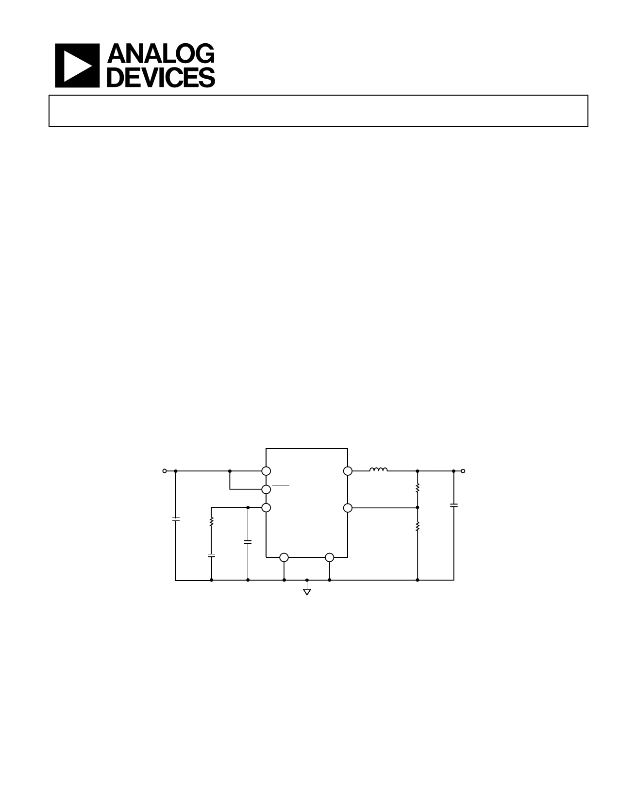
VIN 3.3V
10µF
10kΩ
270pF
TYPICAL APPLICATION CIRCUIT
ADP3051
4 IN
SW 3
7 SHDN
10µH
12.5kΩ
6 COMP
FB 5
27pF
PGND
2
GND
8
10kΩ
VOUT 1.8V
10µF
Figure 1.
Rev. 0
Information furnished by Analog Devices is believed to be accurate and reliable.
However, no responsibility is assumed by Analog Devices for its use, nor for any
infringements of patents or other rights of third parties that may result from its use.
Specifications subject to change without notice. No license is granted by implication
or otherwise under any patent or patent rights of Analog Devices. Trademarks and
registered trademarks are the property of their respective owners.
www.DataSheet4U.com
One Technology Way, P.O. Box 9106, Norwood, MA 02062-9106, U.S.A.
Tel: 781.329.4700
www.analog.com
Fax: 781.326.8703 © 2004 Analog Devices, Inc. All rights reserved.
1 page 
PIN CONFIGURATION AND FUNCTION DESCRIPTIONS
ADP3051
NC 1
8 GND
ADP3051
PGND 2
7 SHDN
SW 3 TOP VIEW 6 COMP
(Not to Scale)
IN 4
5 FB
Figure 2. 8-Lead MSOP Pin Configuration
Table 3. Pin Function Descriptions
Pin No. Mnemonic Description
1 NC
No Connect. Not internally connected.
2 PGND Power Ground. Connect PGND to GND at a single point. Use separate power ground and quiet ground planes for
the power and sensitive analog circuitry, respectively. See the Circuit Board Layout Considerations section.
3 SW
Switching Output. SW connects to the drain of the internal power switch and synchronous rectifier. Connect the
output inductor between SW and the load.
4 IN
Power Source Input. IN is the source of the high side P-channel MOSFET switch, and supplies the internal power to
the ADP3051. Bypass IN to GND with a 0.1 µF or greater ceramic capacitor, placed as close as possible to IN.
5 FB
Feedback Voltage Sense Input. FB senses the output voltage. To set the output voltage, connect a resistive volt-
age divider from the output voltage to FB. The feedback threshold is 0.8 V. See the Setting the Output Voltage
section.
6
COMP
Feedback Loop Compensation Node. COMP is the output of the internal transconductance error amplifier. Place a
series RC network from COMP to GND to compensate the regulator. See the Compensation Design section.
7 SHDN Shutdown Input. Drive SHDN low to turn off the ADP3051; drive SHDN to within 0.5 V of VIN to turn on the
ADP3051. See the Shutdown section.
8 GND
Ground.
Rev. 0 | Page 5 of 16
5 Page 
ADP3051
APPLICATIONS
RECOMMENDED COMPONENTS
External component selection for the application circuit shown
in Figure 20 depends on the load current requirements. Certain
tradeoffs between different performance parameters can also be
made. Recommended external component values are given in
Table 4.
VIN
CIN
ADP3051
4 IN
SW 3
L
7 SHDN
RA
FB 5
8 GND
COMP 6
PGND
2
C2
RB
RC
C1
VOUT
COUT
Figure 20. Typical Application Circuit
DESIGN PROCEDURE
For applications where specific performance is required, com-
ponent combinations other than those listed in Table 4 may be
more appropriate. A design procedure for selecting the compo-
nents is provided in the following sections.
Setting the Output Voltage
The regulated output voltage of the ADP3051 is set by selecting
the resistive voltage divider formed by RA and RB (see
Figure 21). The voltage divider drops the output voltage to the
voltage at FB by the equation
VOUT
=
VFB
⎜⎛1
⎝
+
RA
RB
⎟⎞
⎠
Where VOUT is the output voltage and VFB is the 0.8 V feedback
regulation threshold. RB controls the voltage divider current,
IDIV, which is calculated by
I DIV
= VFB
RB
Using higher divider current increases accuracy due to the 5 nA
FB input bias current. With RB = 100 kΩ, the accuracy is
degraded by 0.0625%.
For a given RB, choose the value of RA to set the output voltage
by the equation
RA
=
RB
⎜⎛
⎝
VOUT
VFB
− 1⎟⎞
⎠
ADP3051
FB
5
VOUT
RA
REF
gm
ERROR
AMPLIFIER
COMP
6
RC
C1
C2
RB
Figure 21. Typical Compensation Network
Table 4. Recommended External Components for Popular Input/Output Voltage Conditions
(Based on ILOAD = 500 mA Max and a 60 kHz Crossover Frequency)
VIN
VOUT
L (µH)
COUT (µF) CIN (µF)
RA (kΩ)
RB (kΩ)
RC (kΩ)
2.5 1.0 6.8 10 10 2.5 10 4.7
1.8 6.8 10 10 12.5 10 10
3.6 1.0 6.8 10 10 2.5 10 4.7
1.8 8.2 10 10 12.5 10 10
2.5 8.2 10 10 21.3 10 15
5.0 1.0 8.2 10 10 2.5 10 5.7
1.8 10 10 10 12.5 10 10
2.5 10 10 10 21.3 10 15
3.3 12 10 10 31.3 10 18
C1 (pF)
470
270
470
270
180
470
270
180
150
C2 (pF)
47
27
47
27
18
47
27
18
15
Rev. 0 | Page 11 of 16
11 Page | ||
| Páginas | Total 16 Páginas | |
| PDF Descargar | [ Datasheet ADP3051.PDF ] | |
Hoja de datos destacado
| Número de pieza | Descripción | Fabricantes |
| ADP3050 | 200 kHz/ 1 A High-Voltage Step-Down Switching Regulator | Analog Devices |
| ADP3051 | PWM Step Down DC-DC | Analog Devices |
| Número de pieza | Descripción | Fabricantes |
| SLA6805M | High Voltage 3 phase Motor Driver IC. |
Sanken |
| SDC1742 | 12- and 14-Bit Hybrid Synchro / Resolver-to-Digital Converters. |
Analog Devices |
|
DataSheet.es es una pagina web que funciona como un repositorio de manuales o hoja de datos de muchos de los productos más populares, |
| DataSheet.es | 2020 | Privacy Policy | Contacto | Buscar |