|
|
PDF GVT71256E18 Data sheet ( Hoja de datos )
| Número de pieza | GVT71256E18 | |
| Descripción | (GVT71256E18 / GVT7C1325A) 256K x 18 Synchronous Flow Through Burst SRAM | |
| Fabricantes | Cypress Semiconductor | |
| Logotipo | ||
Hay una vista previa y un enlace de descarga de GVT71256E18 (archivo pdf) en la parte inferior de esta página. Total 16 Páginas | ||
|
No Preview Available !
( DataSheet : www.DataSheet4U.com )
325A
CY7C1325A/GVT71256E18
256K x 18 Synchronous Flow-Through Burst SRAM
Features
• Fast access times: 7.5 and 8 ns
• Fast clock speed: 117 and 100 MHz
• Provide high-performance 2-1-1-1 access rate
• Fast OE access times: 4.0 ns
• 3.3V –5% and +10% power supply
• 2.5V or 3.3V I/O supply
• 5V tolerant inputs except I/Os
• Clamp diodes to VSSQ at all inputs and outputs
• Common data inputs and data outputs
• Byte Write Enable and Global Write control
• Three chip enables for depth expansion and address
pipeline
• Address, data and control registers
• Internally self-timed Write Cycle
• Burst control pins (interleaved or linear burst se-
quence)
• Automatic power-down for portable applications
• Low profile 119-lead, 14-mm x 22-mm BGA (Ball Grid
Array) and 100-pin TQFP packages
Functional Description
The Cypress Synchronous Burst SRAM family employs high-
speed, low-power CMOS designs using advanced triple-layer
polysilicon, double-layer metal technology. Each memory cell
consists of four transistors and two high-valued resistors.
The CY7C1325A/GVT71256E18 SRAM integrates
262,144x18 SRAM cells with advanced synchronous periph-
eral circuitry and a 2-bit counter for internal burst operation. All
synchronous inputs are gated by registers controlled by a pos-
itive-edge-triggered Clock Input (CLK). The synchronous in-
puts include all addresses, all data inputs, address-pipelining
Chip Enable (CE), depth-expansion Chip Enables (CE2 and
CE2), Burst Control inputs (ADSC, ADSP, and ADV), Write
Enables (WEL, WEH, and BWE), and Global Write (GW).
Asynchronous inputs include the Output Enable (OE) and
Burst Mode Control (MODE), and Sleep Mode Control (ZZ).
The data outputs (DQ), enabled by OE, are also asynchro-
nous.
Addresses and chip enables are registered with either Ad-
dress Status Processor (ADSP) or Address Status Controller
(ADSC) input pins. Subsequent burst addresses can be inter-
nally generated as controlled by the Burst Advance pin (ADV).
Address, data inputs, and write controls are registered on-chip
to initiate a self-timed Write cycle. Write cycles can be one to
four bytes wide as controlled by the write control inputs. Indi-
vidual byte write allows individual byte to be written. WEL con-
trols DQ1–DQ8 and DQP1. WEH controls DQ9–DQ16 and
DQP2. WEL and WEH can be active only with BWE being
LOW. GW being LOW causes all bytes to be written.
The CY7C1325A/GVT71256E18 operates from a +3.3V pow-
er supply and all outputs operate on a +2.5V supply. All inputs
and outputs are JEDEC standard JESD8-5 compatible. The
device is ideally suited for 486, Pentium®, 680x0, and Power-
PC™ systems and for systems that benefit from a wide syn-
chronous data bus.
Selection Guide
Maximum Access Time (ns)
Maximum Operating Current (mA)
Maximum CMOS Standby Current (mA)
7C1325A-117
71256E18-7
7.5
370
10
7C1325A-100
71256E18-8
8
320
10
7C1325A-100
71256E18-9
8
320
10
7C1325A-100
71256E18-10
8
320
10
Pentium is a registered trademark of Intel Corporation.
PowerPC is a trademark of IBM Corporation.
www.DataSheet4U.com
wwCw.yDparteaSssheSeet4mU.iccoomnductor Corporation • 3901 North First Street • San Jose • CA 95134 • 408-943-2600
Document #: 38-05118 Rev. **
Revised September 12, 2001
1 page 
CY7C1325A/GVT71256E18
Pin Descriptions (continued)
BGA Pins
4E
6B
2B
4F
4G
QFP Pins
98
92
97
86
83
4A 84
4B 85
3R 31
7T 64
7P, 6N, 6L, 7K, 58, 59, 62, 63,
6H, 7G, 6F, 7E, 68, 69, 72, 73, 8,
1D, 2E, 2G, 1H, 9, 12, 13, 18, 19,
2K, 1L, 2M, 1N
22, 23
6D, 2P
74, 24
4C, 2J, 4J, 6J, 15, 41,65, 91
4R
3D, 5D, 3E, 5E,
3F, 5F, 5G, 3H,
5H, 3K, 5K, 3L,
3M, 5M, 3N, 5N,
3P, 5P
17, 40, 67, 90
1A, 7A, 1F, 7F, 4, 11, 20, 27, 54,
1J, 7J, 1M, 7M, 61, 70, 77
1U, 7U
5, 10, 21, 26, 55,
60, 71, 76
1B, 7B, 1C, 7C, 1–3, 6, 7, 14, 16,
2D, 4D, 7D, 1E, 25, 28-30, 38,
6E, 2F, 1G, 6G, 39, 42, 43, 51-
2H, 7H, 3J, 5J, 53, 56, 57, 66,
1K, 6K, 2L, 4L, 75, 78, 79, 80,
7L, 6M, 2N, 7N,
95, 96
1P, 6P, 1R, 5R,
7R, 1T, 4T, 2U,
3U, 4U, 5U, 6U
Pin
Name
CE
CE2
CE2
OE
ADV
ADSP
ADSC
MODE
ZZ
DQ1-
DQ16
DQP1,
DQP2
VCC
VSS
VCCQ
VSSQ
NC
Type
Description
Input- Chip Enable: This active LOW input is used to enable the device
Synchronous and to gate ADSP.
Input- Chip Enable: This active LOW input is used to enable the device.
Synchronous
input- Chip Enable: This active HIGH input is used to enable the device.
Synchronous
Input
Output Enable: This active LOW asynchronous input enables the
data output drivers.
Input- Address Advance: This active LOW input is used to control the
Synchronous internal burst counter. A HIGH on this pin generates wait cycle (no
address advance).
Input- Address Status Processor: This active LOW input, along with CE
Synchronous being LOW, causes a new external address to be registered and a
Read cycle is initiated using the new address.
Input- Address Status Controller: This active LOW input causes device to
Synchronous be deselected or selected along with new external address to be
registered. A Read or Write cycle is initiated depending upon write
control inputs.
Input-
Static
Mode: This input selects the burst sequence. A LOW on this pin
selects Linear Burst. A NC or HIGH on this pin selects Interleaved
Burst.
Input- Snooze: This active HIGH input puts the device in low power con-
Asynchro- sumption standby mode. For normal operation, this input has to be
nous either LOW or NC (No Connect).
Input/
Output
Data Inputs/Outputs: Low Byte is DQ1-DQ8. HIgh Byte is DQ9-
DQ16. Input data must meet setup and hold times around the rising
edge of CLK.
Input/
Output
Supply
Parity Inputs/Outputs: DQP1 is parity bit for DQ1-DQ8 and DQP2
is parity bit for DQ9-DQ16.
Power Supply: +3.3V –5% and +10%
Ground Ground: GND
I/O Supply Output Buffer Supply: +2.5V (from 2.375V to VCC)
I/O Ground Output Buffer Ground: GND
- No Connect: These signals are not internally connected.
Document #: 38-05118 Rev. **
Page 5 of 16
5 Page 
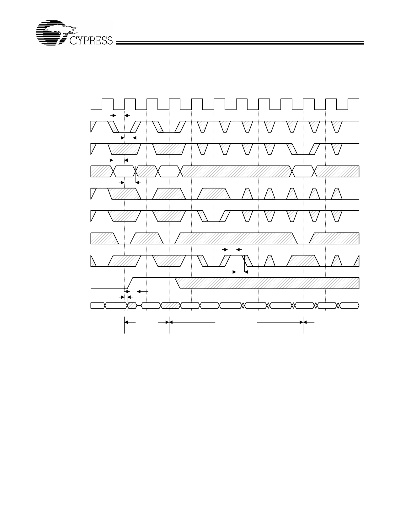
Timing Diagrams (continued)
Write Timing[24]
CY7C1325A/GVT71256E18
CLK
ADSP#
ADSC#
ADDRESS
WEH#, WEL#,
BWE#
GW#
CE#
(See Note)
ADV#
OE#
DQ
tS
tH
tS
A1
tH
A2
A3
tKQX
Q
tOEHZ
D(A1)
SINGLE WRITE
tS
tH
D(A2) D(A2+2) D(A2+2)
D(A2+2)
D(A2+3)
D(A3)
D(A3+1) D(A3+2)
BURST WRITE
BURST WRITE
Document #: 38-05118 Rev. **
Page 11 of 16
11 Page | ||
| Páginas | Total 16 Páginas | |
| PDF Descargar | [ Datasheet GVT71256E18.PDF ] | |
Hoja de datos destacado
| Número de pieza | Descripción | Fabricantes |
| GVT71256E18 | (GVT71256E18 / GVT7C1325A) 256K x 18 Synchronous Flow Through Burst SRAM | Cypress Semiconductor |
| Número de pieza | Descripción | Fabricantes |
| SLA6805M | High Voltage 3 phase Motor Driver IC. |
Sanken |
| SDC1742 | 12- and 14-Bit Hybrid Synchro / Resolver-to-Digital Converters. |
Analog Devices |
|
DataSheet.es es una pagina web que funciona como un repositorio de manuales o hoja de datos de muchos de los productos más populares, |
| DataSheet.es | 2020 | Privacy Policy | Contacto | Buscar |
