|
|
|
PDF MRFIC1803 Data sheet ( Hoja de datos )
| Número de pieza | MRFIC1803 | |
| Descripción | 1.8 GHz UPMIXER / EXCITER AND LO AMP GaAs MONOLITHIC INTEGRATED CIRCUIT | |
| Fabricantes | Motorola Semiconductors | |
| Logotipo | ||
Hay una vista previa y un enlace de descarga de MRFIC1803 (archivo pdf) en la parte inferior de esta página. Total 6 Páginas | ||
|
No Preview Available !
( DataSheet : www.DataSheet4U.com )
MOTOROLA
SEMICONDUCTOR TECHNICAL DATA
Order this document
by MRFIC1803/D
The MRFIC Line
1.8 GHz Upconverter
Designed primarily for use in DECT, Japan’s Personal Handy System (PHS),
and other wireless Personal Communication Systems (PCS) applications at 1.8
GHz, but also applicable to Industrial, Scientific and Medical (ISM) applications
at 2.5 GHz. The MRFIC1803 is a complete active upmixer, exciter amplifier, and
LO buffer amplifier in a low-cost SOIC-16 package. The low power consumption
design includes a single balanced active mixer, CMOS compatible receive and
transmit enable inputs, a buffer/exciter amplifier, and a buffered LO output
capable of driving the MRFIC1804 downconverter. IF, LO and RF ports are
matched to 50 Ω and no off-chip baluns are required. With both TX and RX
enable pins low, the device is in standby mode and draws less than 0.3 mA.
Together with the rest of the MRFIC180X series, this GaAs IC family offers
the complete transmit and receive functions, less LO and filters, needed for a
typical 1.8 GHz cordless telephone.
• 10 dB IF to RF Conversion Gain
• Usable Frequency Range = 1.7 to 2.5 GHz
• Low Power Consumption = 80 mW (Typ)
• Single Bias Supply = 2.7 to 3.3 V
• No External Baluns Required
• IF, LO and RF Ports Matched to 50 Ω
• Low LO Power Requirement = –10 dBm (Typ)
• Low Cost Surface Mount Plastic Package
• Order MRFIC1803R2 for Tape and Reel.
R2 Suffix = 2,500 Units per 16 mm, 13 inch Reel.
• Device Marking = M1803
MAXIMUM RATINGS (TA = 25°C unless otherwise noted)
Ratings
Supply Voltage
IF Input Power
LO Input Power
Transmit and Receive Enable Voltage
Storage Temperature Range
Operating Ambient Temperature
Symbol
VDD
PIF
PLO
TX EN, RX EN
Tstg
TA
MRFIC1803
1.8 GHz UPMIXER,
EXCITER AND LO AMP
GaAs MONOLITHIC
INTEGRATED CIRCUIT
CASE 751B-05
(SO–16)
Value
5.5
3
3
5.5
– 65 to +150
– 30 to + 85
Unit
Vdc
dBm
dBm
Vdc
°C
°C
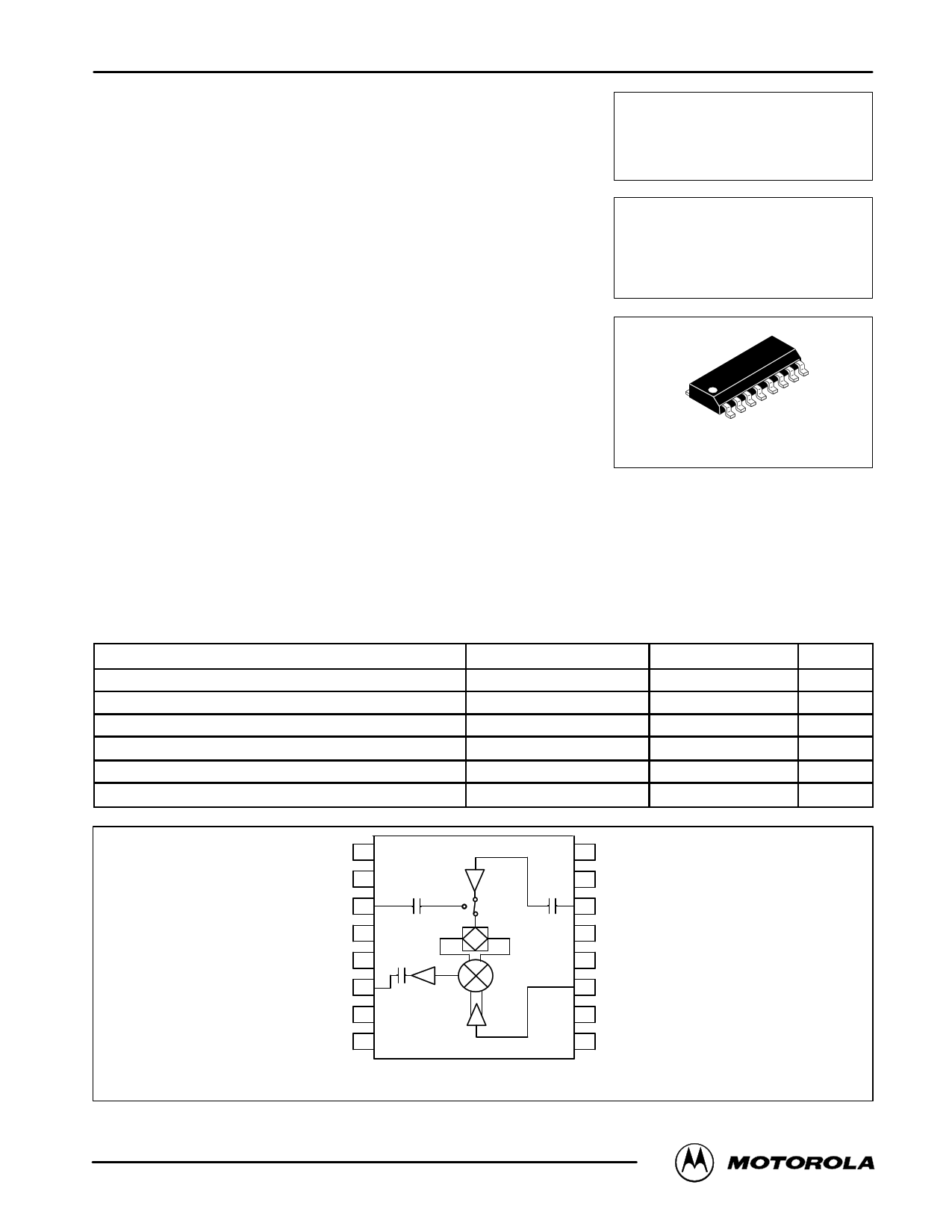
GND 1
GND 2
LO OUT 3
GND 4
GND 5
RF OUT 6
GND 7
VDD 8
LO BUFFER
AND SWITCH
EXCITER
ACTIVE
BALANCED
MIXER
16 RX EN
15 GND
14 LO IN
13 GND
12 GND
11 IF IN
10 GND
9 TX EN
Pin Connections and Functional Block Diagram
REV 3
www©.DMaMtOoatSoTrhOoelaRe,tOI4nUcL..A1c9oR9m7F DEVICE DATA
www.DataSheet4U.com
MRFIC1803
1
1 page 
Frequency (MHz)
1500
1550
1600
1650
1700
1750
1800
1850
1900
1950
2000
2050
2100
2150
2200
2250
2300
2350
2400
2450
2500
RF Output
LO Input
22.07 –j11.36
41.98 +j22.31
21.74 –j4.69
50.60 +j9.80
22.28 +j2.16
41.93 –j0.07
24.01 +j8.25
32.74 +j3.32
26.64 +J14.13
28.78 +j11.39
30.83 +j20.11
28.98 +j21.04
36.39 +j25.30
32.13 +j30.26
43.92 +j29.26
37.68 +j40.38
54.37 +j30.98
48.31 +j54.15
65.34 +j28.57
68.80 +j70.87
75.30 +j21.12
118.18 +j86.46
81.19 +j8.43
220.83 +j17.19
80.22 –j4.24
148.91 –j120.77
74.20 –j14.00
58.50 –j105.11
65.50 –j19.72
27.23 –j71.51
57.40 –j21.38
17.22 –j50.26
50.59 –j20.61
13.00 –j35.19
44.53 –j18.16
10.95 –j22.96
40.24 –j14.78
10.23 –j13.58
37.73 –j10.54
10.20 –j5.32
36.38 –j6.72
10.62 +j2.90
Table 1. Selected Device Impedances
LO Output
20.09 +j31.15
26.39 +j40.79
37.63 +j52.47
56.16 +j63.47
87.97 +j67.31
131.33 +j40.34
137.85 –j16.48
103.88 –j50.81
69.58 –j53.97
50.13 –j46.24
38.97 –j36.86
32.08 –j27.58
28.43 –j19.86
26.56 –j12.82
26.03 –j5.89
26.73 –j0.03
28.46 +j5.10
30.88 +j9.86
33.75 +j13.92
37.50 +j17.32
42.00 +j20.34
DESIGN AND APPLICATIONS INFORMATION
The MRFIC1803 combines a single–balanced FET mix-
er with an LO pre–amp and an exciter amplifier to form a
self–contained upconverter. The device is usable from RF
frequencies of 1.7 to 2.5 GHz and at IF frequencies of 70
to 325 MHz. The design is optimized for low side injection
in hetrodyne transmitter applications. In the upconversion
process, modulation is imparted to an IF carrier which is
converted to the RF transmit frequency by a mixer. By DC
coupling the IF input, the device can be used for simple
on–off keying (OOK) or bi–phase shift keying (BPSK) ap-
plications with no IF.
The MRFIC1803 design minimizes the need for off–chip
components. An active balun is employed at the IF input
and provides an excellent broadband 50W match over the
full range of IF frequencies. The LO quadrature divider is
passive and internal to the device. The LO buffer amplifier
is equipped with a diversity switch which switches the am-
plified LO signal to the LO output pin during RECEIVE
mode. The –5 dBm LO output is the appropriate level to
drive the MRFIC1804 for 1.8 GHz applications or the
MRFIC2401 for 2.4 GHz applications.
As shown in Figure 1, the device is easy to use with
minimal off–chip components. More or less bypassing of
the control and supply lines may be required depending
on board layout and shielding. Careful layout of the RF
frequency portions of the board is critical to successful
implementation. Controlled impedance lines must be used
and any off–chip components must be mounted as close to
the IC as possible. The applications circuit was used to
gather the information displayed in the typical characteris-
tics curves. Since the MRFIC1803 design was optimized
for the 1.7 to 1.9 GHz frequency range, improved perfor-
mance can be had with some off–chip matching at fre-
quencies outside this range. In particular, matching of the
LO port will supply higher LO drive and improve conver-
sion gain. At the RF output, either better gain or better 1dB
compression can be had with external matching.
Filtering is generally required in the upconversion pro-
cess to reduce image and LO radiation. To minimize pin
count, this filtering is accomplished external to the device
at the exciter output. For the frequency ranges of applica-
tion, two and three pole ceramic surface filters are avail-
able at reasonable cost and with less than 2 dB of loss.
EVALUATION BOARDS
Evaluation boards are available for RF Monolithic Inte-
grated Circuits by adding a “TF” suffix to the device type.
For a complete list of currently available boards and ones
in development for newly introduced product, please con-
tact your local Motorola Distributor or Sales Office.
MOTOROLA RF DEVICE DATA
MRFIC1803
5
5 Page | ||
| Páginas | Total 6 Páginas | |
| PDF Descargar | [ Datasheet MRFIC1803.PDF ] | |
Hoja de datos destacado
| Número de pieza | Descripción | Fabricantes |
| MRFIC1801 | 1.8 GHz TRANSMIT/RECEIVE ANTENNA SWITCH GaAs MONOLITHIC INTEGRATED CIRCUIT | Motorola Semiconductors |
| MRFIC1803 | 1.8 GHz UPMIXER / EXCITER AND LO AMP GaAs MONOLITHIC INTEGRATED CIRCUIT | Motorola Semiconductors |
| MRFIC1804 | 1.8 GHz LOW NOISE AMPLIFIER AND DOWNMIXER GaAs MONOLITHIC INTEGRATED CIRCUIT | Motorola Semiconductors |
| MRFIC1805 | 1.9 GHz POWER AMPLIFIER GaAs MONOLITHIC INTEGRATED CIRCUIT | Motorola Semiconductors |
| Número de pieza | Descripción | Fabricantes |
| SLA6805M | High Voltage 3 phase Motor Driver IC. |
Sanken |
| SDC1742 | 12- and 14-Bit Hybrid Synchro / Resolver-to-Digital Converters. |
Analog Devices |
|
DataSheet.es es una pagina web que funciona como un repositorio de manuales o hoja de datos de muchos de los productos más populares, |
| DataSheet.es | 2020 | Privacy Policy | Contacto | Buscar |