|
|
|
PDF MRFIC1804 Data sheet ( Hoja de datos )
| Número de pieza | MRFIC1804 | |
| Descripción | 1.8 GHz LOW NOISE AMPLIFIER AND DOWNMIXER GaAs MONOLITHIC INTEGRATED CIRCUIT | |
| Fabricantes | Motorola Semiconductors | |
| Logotipo | ||
Hay una vista previa y un enlace de descarga de MRFIC1804 (archivo pdf) en la parte inferior de esta página. Total 6 Páginas | ||
|
No Preview Available !
( DataSheet : www.DataSheet4U.com )
MOTOROLA
SEMICONDUCTOR TECHNICAL DATA
The MRFIC Line
1.8 GHz LNA/Downmixer
Designed primarily for use in DECT, Japan Personal Handy Phone (JPHP),
and other wireless Personal Communication Systems (PCS) applications. The
MRFIC1804 includes a low noise amplifier and downmixer in a low-cost
SOIC-16 package. The integrated circuit requires minimal off-chip matching
while allowing for the maximum in flexibility and efficiency. The mixer is
optimized for low side injection and offers reasonable intercept point as well as
high efficiency and 4 dB of conversion gain. Image filtering is implemented
off-chip to allow maximum flexibility. With both TX and RX enable pins low, the
device is in standby mode and draws less than 0.5 mA.
Together with the rest of the MRFIC180X series, this GaAs IC family offers
the complete transmit and receive functions, less LO and filters, needed for a
typical 1.8 GHz cordless telephone.
• Usable Frequency Range = 1.5 to 2.2 GHz
• 14 dB Gain, 2.3 dB Noise Figure LNA
• 4 dB Gain, 13 dB Noise Figure Mixer
• 0.9 dB Mixer Input Intercept Point
• Simple LO/IF Off-Chip Matching for Maximum Flexibility
• Low Power Consumption = 24 mW (Typ)
• Single Bias Supply = 2.7 to 3.3 V
• Low LO Power Requirement = – 5 dBm (Typ)
• Low Cost Surface Mount Plastic Package
• Available in Tape and Reel by Adding R2 Suffix to Part Number.
R2 Suffix = 2,500 Units per 16 mm, 13 inch Reel.
• Device Marking = M1804
Order this document
by MRFIC1804/D
MRFIC1804
1.8 GHz LOW NOISE
AMPLIFIER AND
DOWNMIXER
GaAs MONOLITHIC
INTEGRATED CIRCUIT
CASE 751B-05
(SO–16)
VDD 1
GND 2
RF IN 3
GND 4
GND 5
LNA OUT 6
GND 7
RX EN 8
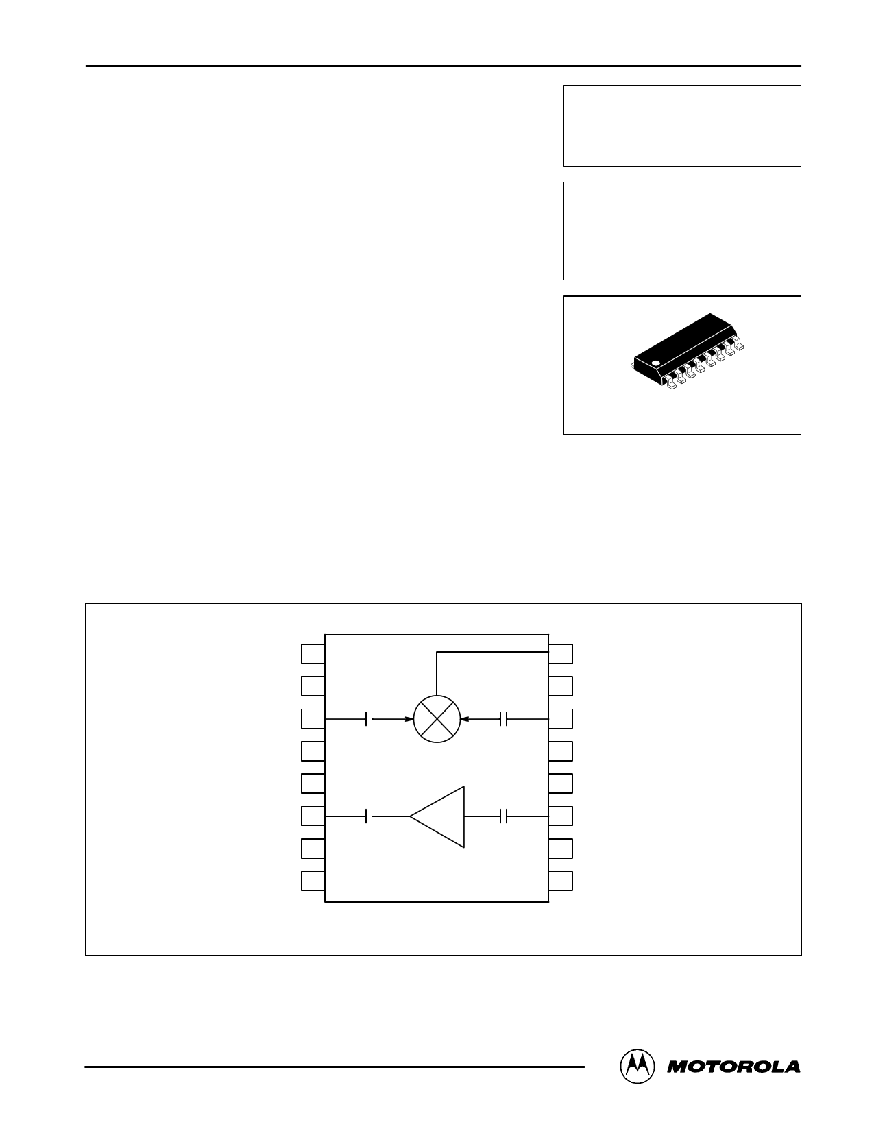
MIXER
LNA
16 IF OUT/VDD
15 GND
14 LO IN
13 GND
12 GND
11 LNA IN
10 GND
9 VDD
Pin Connections and Functional Block Diagram
REV 2
www©.DMaMtOoatSoTrhOoelaRe,tOI4nUcL..A1c9oR9m5F DEVICE DATA
www.DataSheet4U.com
MRFIC1804
1
1 page 
DESIGN AND APPLICATIONS INFORMATION
The MRFIC1804 consists of a two–stage GaAs MESFET
low noise amplifier and a single ended MESFET mixer. The
LNA design conserves bias current through stacking of the
two FETs, thus reusing the current. The mixer consists of a
common gate stage driving a common source stage with
the IF output being the drain of the common source stage
shunted with 15 pF. The LNA output and mixer input have
been separated to allow the addition of an external image
filter. Such a filter, usually ceramic, is useful in improving
the mixer noise figure and third order intercept perfor-
mance. It also provides LO rejection to reduce the amount
of LO power which may leak to the antenna. Alternatively,
image trapping can be implemented at the LNA input or out-
put with discrete or distributed components.
The design has been optimized for application in the PCS
bands around 1.9 GHz but is usable from around 1.5 GHz to
2.2 GHz. For applications at 1.9 GHz and IFs of 110 MHz or
240 MHz, the circuit shown in Figure 1 can be used. This
circuit was used to derive the characterization data shown
in Figures 3 through 8. For other IF frequencies in the 100
MHz to 350 MHz range, use the IF equivalent circuit shown
in Figure 2 for matching network design. As can be seen in
the characterization curves, performance appears to de-
grade above about 1.85 GHz. This is partially a function of
the circuit shown in Figure 1 and can be improved, first, by
adjusting the LO input match, second, by matching LNA in-
put and and the mixer input off chip.
As with all RF circuits, layout is important. Ground vias
must be close to the component or lead to be grounded and
vias must be plentiful. RF signal lines should be controlled
impedance such as microstrip. Bypassing of power supply
leads as shown in Figure 1 is essential to avoid oscillation of
the circuits.
EVALUATION BOARDS
Evaluation boards are available for RF Monolithic Inte-
grated Circuits by adding a “TF” suffix to the device type.
For a complete list of currently available boards and ones
in development for newly introduced poduct, please con-
tact your local Motorola Distributor or Sales Office.
MOTOROLA RF DEVICE DATA
MRFIC1804
5
5 Page | ||
| Páginas | Total 6 Páginas | |
| PDF Descargar | [ Datasheet MRFIC1804.PDF ] | |
Hoja de datos destacado
| Número de pieza | Descripción | Fabricantes |
| MRFIC1801 | 1.8 GHz TRANSMIT/RECEIVE ANTENNA SWITCH GaAs MONOLITHIC INTEGRATED CIRCUIT | Motorola Semiconductors |
| MRFIC1803 | 1.8 GHz UPMIXER / EXCITER AND LO AMP GaAs MONOLITHIC INTEGRATED CIRCUIT | Motorola Semiconductors |
| MRFIC1804 | 1.8 GHz LOW NOISE AMPLIFIER AND DOWNMIXER GaAs MONOLITHIC INTEGRATED CIRCUIT | Motorola Semiconductors |
| MRFIC1805 | 1.9 GHz POWER AMPLIFIER GaAs MONOLITHIC INTEGRATED CIRCUIT | Motorola Semiconductors |
| Número de pieza | Descripción | Fabricantes |
| SLA6805M | High Voltage 3 phase Motor Driver IC. |
Sanken |
| SDC1742 | 12- and 14-Bit Hybrid Synchro / Resolver-to-Digital Converters. |
Analog Devices |
|
DataSheet.es es una pagina web que funciona como un repositorio de manuales o hoja de datos de muchos de los productos más populares, |
| DataSheet.es | 2020 | Privacy Policy | Contacto | Buscar |