|
|
|
PDF LM5035 Data sheet ( Hoja de datos )
| Número de pieza | LM5035 | |
| Descripción | PWM Controller with Integrated Half-Bridge and SyncFET Drivers | |
| Fabricantes | National Semiconductor | |
| Logotipo | ||
Hay una vista previa y un enlace de descarga de LM5035 (archivo pdf) en la parte inferior de esta página. Total 28 Páginas | ||
|
No Preview Available !
www.DataSheet4U.com
January 2006
LM5035
PWM Controller with Integrated Half-Bridge and
SyncFET Drivers
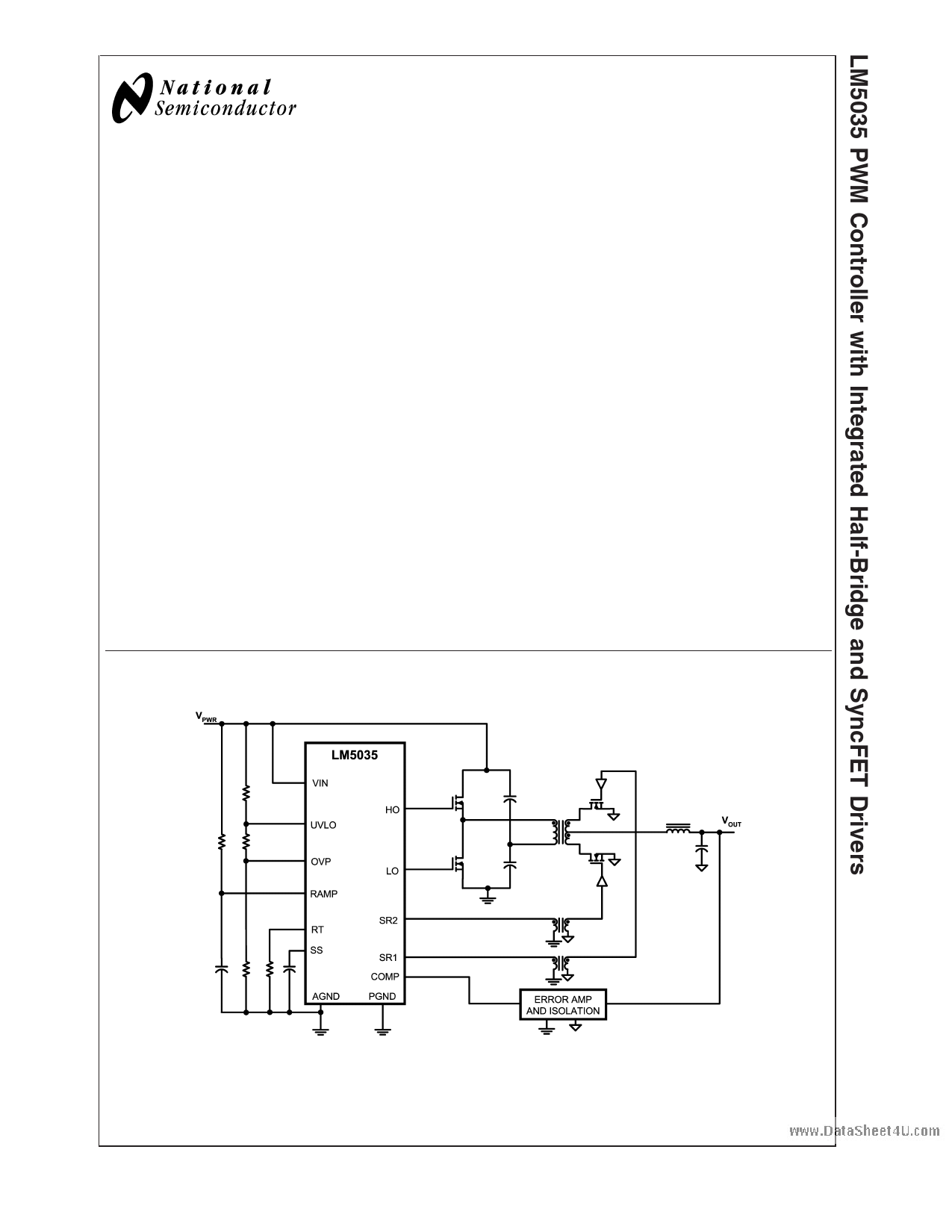
General Description
The LM5035 Half-Bridge Controller/Gate Driver contains all
of the features necessary to implement half-bridge topology
power converters using voltage mode control with line volt-
age feed-forward. The floating high-side gate driver is ca-
pable of operating with supply voltages up to 105V. Both the
high-side and low-side gate drivers are capable of 2A peak.
An internal high voltage startup regulator is included, along
with programmable line undervoltage lockout (UVLO) and
overvoltage protection (OVP). The oscillator is programmed
with a single resistor to frequencies up to 2MHz. The oscil-
lator can also be synchronized to an external clock. A current
sense input and a programmable timer provide cycle-by-
cycle current limit and adjustable hiccup mode overload
protection.
Features
n 105V / 2A Half-Bridge Gate Drivers
n Synchronous Rectifier Control Outputs with
Programmable Delays
n High Voltage (105V) Start-up Regulator
n Voltage mode Control with Line Feed-Forward and Volt •
Second Limiting
n Resistor Programmed, 2MHz Capable Oscillator
n Patent Pending Oscillator Synchronization
n Programmable Line Under-Voltage Lockout
n Line Over-Voltage Protection
n Internal Thermal Shutdown Protection
n Adjustable Soft-Start
n Versatile Dual Mode Over-Current Protection with
Hiccup Delay Timer
n Cycle-by-Cycle Over-Current Protection
n Direct Opto-coupler Interface
n 5V Reference Output
Packages
www.DataSheet4U.comn TSSOP-20EP (Thermally enhanced)
n LLP-24 (4mm x 5mm)
Simplified Application Diagram
© 2006 National Semiconductor Corporation DS201775
DataSheet4 U .com
20177501
www.national.com
www.DataSheet4U.com
1 page 
www.DataSheet4U.com
Absolute Maximum Ratings (Note 1)
If Military/Aerospace specified devices are required,
please contact the National Semiconductor Sales Office/
Distributors for availability and specifications.
VIN to GND
HS to GND
HB to GND
HB to HS
VCC to GND
CS, RT, DLY to GND
COMP Input Current
-0.3V to 105V
-1V to 105V
-0.3V to 118V
-0.3V to 18V
-0.3V to 16V
-0.3V to 5.5V
10mA
All other inputs to GND
ESD Rating (Note 4)
Human Body Model
Storage Temperature Range
Junction Temperature
-0.3V to 7V
2kV
-65˚C to 150˚C
150˚C
Operating Ratings (Note 1)
VIN Voltage
External Voltage Applied to VCC
Operating Junction Temperature
13V to 105V
8V to 15V
-40˚C to +125˚C
Electrical Characteristics Specifications with standard typeface are for TJ = 25˚C, and those with boldface
type apply over full Operating Junction Temperature range. VVIN = 48V, VVCC = 10V externally applied, RRT = 15.0 kΩ,
RDLY = 27.4kΩ, VUVLO = 3V, VOVP = 0V unless otherwise stated. See (Note 2) and (Note 3).
Symbol Parameter
Conditions
Min Typ
Startup Regulator (VCC pin)
VVCC
IVCC(LIM)
VVCCUV
VCC voltage
VCC current limit
VCC Under-voltage threshold
(VCC increasing)
IVCC = 10mA
VVCC = 7V
VIN = VCC, ∆VVCC from the regulation
setpoint
7.3 7.6
20 25
0.2 0.1
VCC decreasing
VCC – PGND
5.5 6.2
IVIN Startup regulator current
VIN = 90V, UVLO = 0V
Supply current into VCC from
Outputs & COMP open, VVCC = 10V,
external source
Outputs Switching
30
4
Voltage Reference Regulator (REF pin)
www.DataSheet4U.comVREF
REF Voltage
REF Voltage Regulation
IREF = 0mA
IREF = 0 to 10mA
4.85
5
25
REF Current Limit
REF = 4.5V
15 20
Under-Voltage Lock Out and shutdown (UVLO pin)
VUVLO
IUVLO
Under-voltage threshold
Hysteresis current
UVLO pin sinking
Under-voltage Shutdown Threshold UVLO voltage falling
1.212
19
1.25
23
0.3
Under-voltage Standby Enable
UVLO voltage rising
0.4
Threshold
Over-Voltage Protection (OVP pin)
VOVP
Over-Voltage threshold
IOVP
Hysteresis current
Current Sense Input (CS Pin)
OVP pin sourcing
1.212 1.25
19 23
VCS Current Limit Threshold
CS delay to output
0.228 0.25
CS from zero to 1V. Time for HO and LO
80
to fall to 90% of VCC. Output load = 0
pF.
Leading edge blanking time at CS
50
CS sink impedance (clocked)
Internal FET sink impedance
32
Current Limit Restart (RES Pin)
VRES
RES Threshold
Charge source current
Discharge sink current
VRES = 1.5V
VRES = 1V
2.4 2.5
16 22
8 12
Max
7.9
6.9
70
6
5.15
50
1.288
27
1.288
27
0.272
60
2.6
28
16
Units
V
mA
V
V
µA
mA
V
mV
mA
V
µA
V
V
V
µA
V
ns
ns
Ω
V
µA
µA
DataSheet4 U .com
5 www.national.com
www.DataSheet4U.com
5 Page 
www.DataSheet4U.com
Functional Description
The LM5035 PWM controller contains all of the features
necessary to implement half-bridge voltage-mode controlled
both the VCC and the VIN pins. The external bias must be
greater than 8.3V to exceed the VCC UVLO threshold and
less than the VCC maximum operating voltage rating (15V).
power converters. The LM5035 provides two gate driver
outputs to directly drive the primary side power MOSFETs
Line Under-Voltage Detector
and two signal level outputs to control secondary synchro-
The LM5035 contains a dual level Under-Voltage Lockout
nous rectifiers through an isolation interface. Secondary side
(UVLO) circuit. When the UVLO pin voltage is below 0.4V,
drivers, such as the LM5110, are typically used to provide
the controller is in a low current shutdown mode. When the
the necessary gate drive current to control the sync MOS-
UVLO pin voltage is greater than 0.4V but less than 1.25V,
FETs. Synchronous rectification allows higher conversion
the controller is in standby mode. In standby mode the VCC
efficiency and greater power density than conventional PN or
and REF bias regulators are active while the controller out-
Schottky rectifier techniques. The LM5035 can be configured
puts are disabled. When the VCC and REF outputs exceed
to operate with bias voltages ranging from 8V to 105V.
the VCC and REF under-voltage thresholds and the UVLO
Additional features include line under-voltage lockout, cycle-
pin voltage is greater than 1.25V, the outputs are enabled
by-cycle current limit, voltage feed-forward compensation,
and normal operation begins. An external set-point voltage
hiccup mode fault protection with adjustable delays, soft-
divider from VIN to GND can be used to set the minimum
start, a 2MHz capable oscillator with synchronization capa-
operating voltage of the converter. The divider must be
bility, precision reference, thermal shutdown and program-
designed such that the voltage at the UVLO pin will be
mable volt•second clamping. These features simplify the
greater than 1.25V when VIN enters the desired operating
design of voltage-mode half-bridge DC-DC power convert-
range. UVLO hysteresis is accomplished with an internal
ers. The Functional Block Diagram is shown in Figure 1.
23uA current sink that is switched on or off into the imped-
ance of the set-point divider. When the UVLO threshold is
High-Voltage Start-up Regulator
exceeded, the current sink is deactivated to quickly raise the
voltage at the UVLO pin. When the UVLO pin voltage falls
The LM5035 contains an internal high voltage start-up regu-
below the 1.25V threshold, the current sink is enabled caus-
lator that allows the input pin (VIN) to be connected directly
ing the voltage at the UVLO pin to quickly fall. The hysteresis
to a nominal 48 VDC input voltage. The regulator input can
of the 0.4V shutdown comparator is internally fixed at
withstand transients up to 105V. The regulator output at VCC
100mV.
(7.6V) is internally current limited to 25 mA typical. When the
UVLO pin potential is greater than 0.4V, the VCC regulator is
enabled to charge an external capacitor connected to the
VCC pin. The VCC regulator provides power to the voltage
reference (REF) and the output drivers (LO, SR1 and SR2).
When the voltage on the VCC pin exceeds the UVLO thresh-
www.DataSheet4U.comold of 7.6V, the internal voltage reference (REF) reaches its
regulation setpoint of 5V and the UVLO voltage is greater
The UVLO pin can also be used to implement various re-
mote enable / disable functions. Turning off a converter by
forcing the UVLO pin to the standby condition provides a
controlled soft-stop. See the Soft Start section for more
details.
Line Over Voltage / Load Over
than 1.25V, the controller outputs are enabled. The value of
the VCC capacitor depends on the total system design, and
its start-up characteristics. The recommended range of val-
Voltage / Remote Thermal
Protection
ues for the VCC capacitor is 0.1µF to 100µF.
The LM5035 provides a multipurpose OVP pin that supports
The VCC under-voltage comparator threshold is lowered to
several fault protection functions. When the OVP pin voltage
6.2V (typical) after VCC reaches the regulation set-point. If
exceeds 1.25V, the controller is held in standby mode which
VCC falls below this value, the outputs are disabled, and the
immediately halts the PWM pulses at the HO and LO pins. In
soft-start capacitor is discharged. If VCC increases above
standby mode, the VCC and REF bias regulators are active
7.6V, the outputs will be enabled and a soft-start sequence
while the controller outputs are disabled. When the OVP pin
will commence.
voltage falls below the 1.25V OVP threshold, the outputs are
The internal power dissipation of the LM5035 can be re-
duced by powering VCC from an external supply. In typical
applications, an auxiliary transformer winding is connected
through a diode to the VCC pin. This winding must raise the
VCC voltage above 8.3V to shut off the internal start-up
regulator. Powering VCC from an auxiliary winding improves
efficiency while reducing the controller’s power dissipation.
The under-voltage comparator circuit will still function in this
enabled and normal soft-start sequence begins. Hysteresis
is accomplished with an internal 23µA current source that is
switched on or off into the impedance of the OVP pin set-
point divider. When the OVP threshold is exceeded, the
current source is enabled to quickly raise the voltage at the
OVP pin. When the OVP pin voltage falls below the 1.25V
threshold, the current source is disabled causing the voltage
at the OVP pin to quickly fall.
mode, requiring that VCC never falls below 6.2V during the
Several examples of the use of this pin are provided in the
start-up sequence.
Application Information section.
During a fault mode, when the converter auxiliary winding is
inactive, external current draw on the VCC line should be
limited such that the power dissipated in the start-up regula-
tor does not exceed the maximum power dissipation of the
IC package.
An external DC bias voltage can be used instead of the
internal regulator by connecting the external bias voltage to
Reference
The REF pin is the output of a 5V linear regulator that can be
used to bias an opto-coupler transistor and external house-
keeping circuits. The regulator output is internally current
limited to 20mA (typical).
DataSheet 4 U .com
11 www.national.com
www.DataSheet4U.com
11 Page | ||
| Páginas | Total 28 Páginas | |
| PDF Descargar | [ Datasheet LM5035.PDF ] | |
Hoja de datos destacado
| Número de pieza | Descripción | Fabricantes |
| LM5030 | 100V Push-Pull Current Mode PWM Controller | National Semiconductor |
| LM5030 | LM5030 100-V Push-Pull Current Mode PWM Controller (Rev. D) | Texas Instruments |
| LM5030MM | 100V Push-Pull Current Mode PWM Controller | National Semiconductor |
| LM5030MMX | 100V Push-Pull Current Mode PWM Controller | National Semiconductor |
| Número de pieza | Descripción | Fabricantes |
| SLA6805M | High Voltage 3 phase Motor Driver IC. |
Sanken |
| SDC1742 | 12- and 14-Bit Hybrid Synchro / Resolver-to-Digital Converters. |
Analog Devices |
|
DataSheet.es es una pagina web que funciona como un repositorio de manuales o hoja de datos de muchos de los productos más populares, |
| DataSheet.es | 2020 | Privacy Policy | Contacto | Buscar |