|
|
|
PDF ISPPAC30 Data sheet ( Hoja de datos )
| Número de pieza | ISPPAC30 | |
| Descripción | In-System Programmable Analog Circuit | |
| Fabricantes | Lattice Semiconductor | |
| Logotipo | ||
Hay una vista previa y un enlace de descarga de ISPPAC30 (archivo pdf) en la parte inferior de esta página. Total 30 Páginas | ||
|
No Preview Available !
www.DataSheet4U.com
ispPAC30
In-System Programmable Analog Circuit
October 2002
Data Sheet
Features
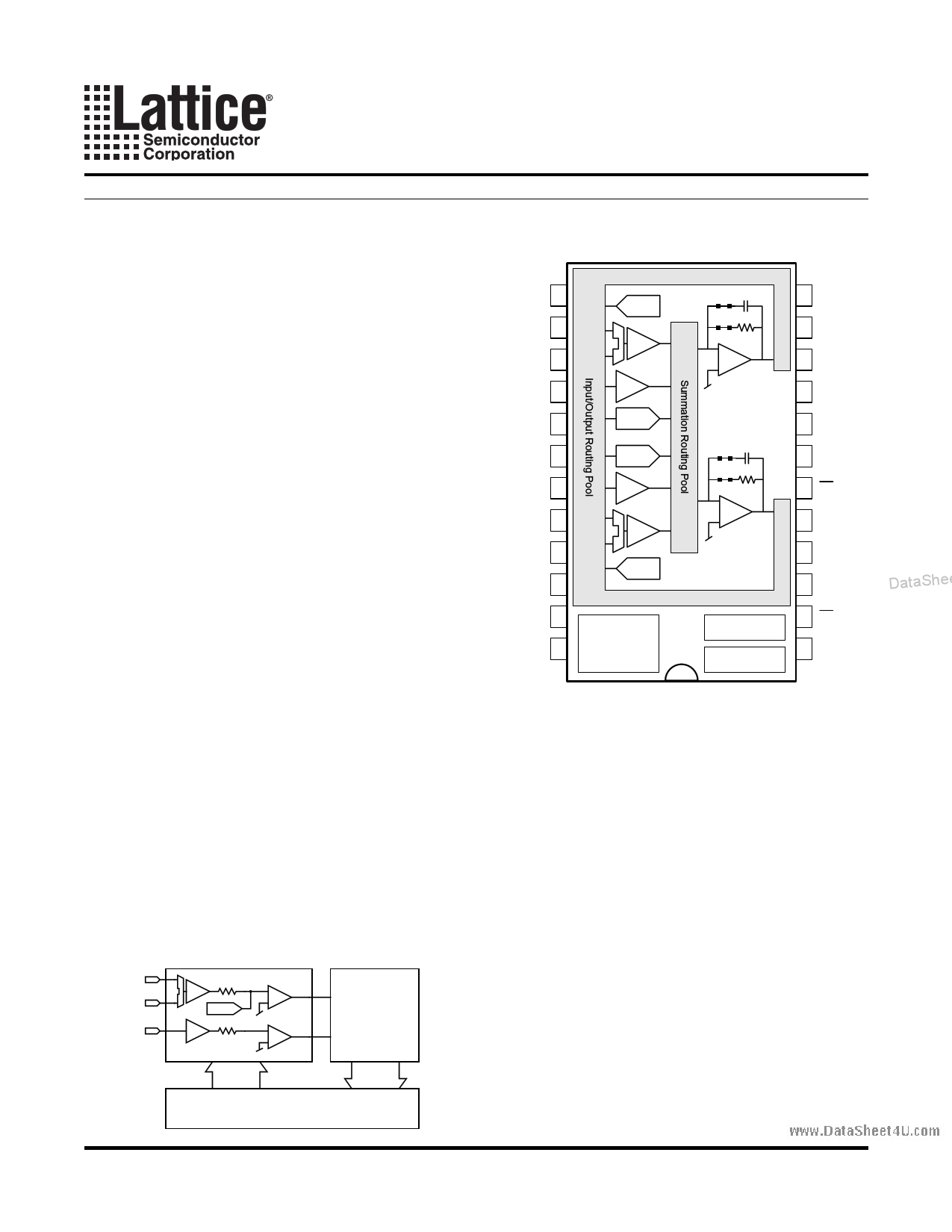
Functional Block Diagram
■ Flexible Interface and Programming Control
• Full configuration capability, SPI or JTAG modes
• Unlimited device updates using SRAM register
• E2CMOS® for non-volatile configuration storage
• Real-time microcontroller configuration/control
■ Four Input Instrumentation Amplifiers (IA’s)
• High impedance: differential or single-ended
• 0V to 2.8V with programmable gains (±1 to ±10)
• Dual multiplexers (pin or serial port controlled)
• Connects easily to existing system circuits
IN1+ 13
IN1- 14
IN2+ 15
IN2- 16
VREFOUT 17
Vref1
IA
IA
MDAC
OA
Filter
Amplify
Integrate
Compare
12 VS
11 ENSPI
10 TMS
9 TDO
8 TDI
■ Two Configurable Rail-to-Rail Output Amps
• Single-ended, 0V to 5V output swing
• Gain bandwidth product >15MHz
• Amplifier, filter, integrator or comparator modes
• 7 filter frequencies (50kHz to 600kHz)
OUT1 18
OUT2 19
SCOM 20
■ Two 4-Quadrant, 8-Bit Multiplying DACs
IN3+ 21
• Full bandwidth when used as a multiplier
• Precision gain (<0.01 steps) with signal as input
IN3- 22
• Precision offset (in 7 ranges) using internDaal tVarSehf eet4U.coINm4+ 23
■ Analog Input/Summation Routing Pools
• Routing of all I/O to any IA or MDAC
IN4- 24
• Any IA/MDAC summed to either output amplifier
• Circuits with and without feedback possible
• Routable to maintain pin location relationships
MDAC
IA
IA
Vref2
OA
Filter
Amplify
Integrate
Compare
JTAG/SPI
Interface Logic
& Configuration
Memory
Auto-Calibration
2.5V Reference
ispPAC30 24-Pin SOIC
7 TCK
6 CS
5 MSEL1
4 MSEL2
3 CAL
2 PD
1 GND
■ Other Product Features
• Single supply (+5V) operation
• Precision voltage reference output (2.5V)
• Power-down for µWatt power consumption
• Auto-calibration of internal offsets
• Available in 28-pin PDIP or 24-pin SOIC
■ Applications
• Reconfigurable or adaptive signal conditioning
• Analog front end for most A/D converters
• Programmable analog signal control loops
• Precision programmable gain amplifiers
Vin1
Vin2
Vin3
ispPAC30
Dual
12-Bit
ADC
DataSheet4U.com
µController
Description
The ispPAC®30 is a member of the Lattice family of In-
System Programmable (ISP™) analog integrated cir-
cuits. It is digitally configured via SRAM and utilizes
E2CMOS memory for non-volatile storage of its configu-
ration. The flexibility of ISP enables programming, verifi-
cation and unlimited reconfiguration, directly on the
printed circuit board.
The ispPAC30 is a complete front end solution for data
acquisition applications using 10 to 12-bit ADC's. It pro-
vides multiple single-ended or differential signal inputs,
multiplexing, precision gain, offset adjustment, filtering,
and comparison functionality. It also has complete
routability of inputs or outputs to any input cell and then
from any input cell to either summing node of the two
output amplifiers. Designers configure the ispPAC30
and verify its performance using PAC-Designer®, an
easy to use, Microsoft Windows® compatible develop-
ment tool. Device programming is supported using PC
parallel port I/O operations.
DataShee
www.latticesemi.com
1
pac30_01
DataSheet4 U .com
DataSheet4U.com
1 page 
www.DataSheet4U.com
Lattice Semiconductor
ispPAC30 Data Sheet
Pin Descriptions
et4U.com
Pins
PDIP
SOIC
15, 16, 17, 18, 13, 14, 15, 16,
25, 26, 27, 28 21, 22, 23, 24
65
4
21, 22
20
13
12
11
9
8
7
3
2
14
1
23
5, 10, 19, 24
4
18, 19
17
11
10
9
8
7
6
3
2
12
1
20
—
Symbol
IN
MSEL1
MSEL2
OUT
VREFOUT
ENSPI
TMS
TDO
TDI
TCK
CS
CAL
PD
VS
GND
SCOM
NC
Name
Description
Inputs 1, 2, 3, 4 (+ or -)
Plus or Minus
Multiplexer 1 Control
Differential input pins, with two pins per input
(e.g., IN2+ and IN2-). Each are components of
VIN, where differential VIN = VIN+ - VIN-.
Multiplexer logic input pin. Selects either of two
analog channels to IA1 (instrument amplifier).
Programmable pull-up, pull-down (default), or
none.
Multiplexer 2 Control
Multiplexer logic input pin. Selects either of two
analog channels to IA4 (instrument amplifier).
Programmable pull-up, pull-down (default), or
none.
Outputs 1 and 2
Single-ended output pins. Internal feedback to
inputs accommodated.
Internal voltage reference output pin (+2.5V
Voltage Reference Output nominal). Must be bypassed to GND with a 1µF
capacitor.
Enable SPI Mode
Enable SPI logic input pin. When high, causes
serial port to run in SPI mode. Programmable
pull-up or pull-down (default).
Test Mode Select
Serial interface logic mode select pin (input).
JTAG interface mode only. Internal pull-up.
Test Data Out
DataSheet4U.com
Test Data In
Serial interface logic pin (output) for both JTAG
and SPI operation modes. Programmable slew
rate, high or low (default).
Serial interface logic pin (input) for both JTAG
and SPI modes. Internal pull-up.
Test Clock
Serial interface logic clock pin (input) for both
JTAG and SPI modes. Programmable pull-up,
pull-down (default), or none.
Chip Select
Chip select logic input pin. SPI data transfer
enabled by this input. Internal pull-up.
Auto-Calibrate
Digital pin (input). Commands an auto-calibration
sequence on a rising edge. Internal pull-down.
Power Down
Power down enable logic pin (input). Shuts down
all power to device. Programmable pull-up
(default), pull-down or none.
Supply Voltage
Analog supply pin (5V nominal). Should be
bypassed to GND with 1µF and .01µF capaci-
tors.
Ground
Ground pin. Should normally be connected to
the analog ground plane.
Signal Common
Analog signal common pin (sense). Always con-
nected to GND. Auto-calibration accuracy is
determined with respect to this pin.
No Connects
No internal connections are made to these pins
in the PDIP package.
DataShee
DataSheet4U.com
DataSheet4 U .com
5
DataSheet4U.com
5 Page 
www.DataSheet4U.com
Lattice Semiconductor
ispPAC30 Data Sheet
Typical Performance Characteristics
Input Noise Spectrum
1000
CMR vs. Frequency
90
80
PSR vs. Frequency
90
80
70 70
100
Noise: Referred to Input
G = 10
10
1
10 100 1k 10k 100k 1M
Frequency (Hz)
60
50
40
30
10
100 1k 10k 100k 1M
Frequency (Hz)
60
50
40
30
100
1k 10k 100k 1M
Frequency (Hz)
et4U.com
Small Signal BW vs. Gain
25
20
Gain = 10
15
10 Gain = 5
-5 Gain = 2
0
Gain = 1
-5
-10
-15
-20
-25
1k
10k 100k 1M
Frequency (Hz)
10M
THD vs. Frequency
-40
-50
-60
DataSheeGt4aUin.=co10m
-70
-80
Gain = 1
-90
-100
1k
10k
Frequency (Hz)
100k
Output Current Drive
75
Vout Forced to
50 Nominal - 50mV
25
DataShee
0
-25 Vout Forced to
Nominal + 50mV
-50
-75
0
12
34
Nominal Output Voltage (V)
5
Gain Error (Gain = 1 & 10)
40
3 Wafer Lots
35
PDIP Pkg
0°C to +85°C
30
25
20
15
10
5
0
-1.8 -1.0 -.2 +.2 +1.0 +1.8
Gain Error (%)
DataSheet4U.com
DataSheet4 U .com
Offset Voltage (VOS)
30
3 Wafer Lots
25
PDIP Pkg
+25°C
20
For All Gains,
Output Referred
15
10
5
0
-2 -1 0 +1 +2
Offset (mV)
VOS Tempco
30
3 Wafer Lots
25
PDIP Pkg
-40°C to +85°C
20
15
10
5
0
-100 -50
0 +50 +100
Offset Tempco (µV/°C)
11
DataSheet4U.com
11 Page | ||
| Páginas | Total 30 Páginas | |
| PDF Descargar | [ Datasheet ISPPAC30.PDF ] | |
Hoja de datos destacado
| Número de pieza | Descripción | Fabricantes |
| ISPPAC30 | In-System Programmable Analog Circuit | Lattice Semiconductor |
| Número de pieza | Descripción | Fabricantes |
| SLA6805M | High Voltage 3 phase Motor Driver IC. |
Sanken |
| SDC1742 | 12- and 14-Bit Hybrid Synchro / Resolver-to-Digital Converters. |
Analog Devices |
|
DataSheet.es es una pagina web que funciona como un repositorio de manuales o hoja de datos de muchos de los productos más populares, |
| DataSheet.es | 2020 | Privacy Policy | Contacto | Buscar |