|
|
|
PDF ISPPAC81 Data sheet ( Hoja de datos )
| Número de pieza | ISPPAC81 | |
| Descripción | In-System Programmable Analog Circuit | |
| Fabricantes | Lattice Semiconductor | |
| Logotipo | ||
Hay una vista previa y un enlace de descarga de ISPPAC81 (archivo pdf) en la parte inferior de esta página. Total 20 Páginas | ||
|
No Preview Available !
www.DataSheet4U.com
ispPAC81
In-System Programmable Analog Circuit
October 2001
Data Sheet
Features
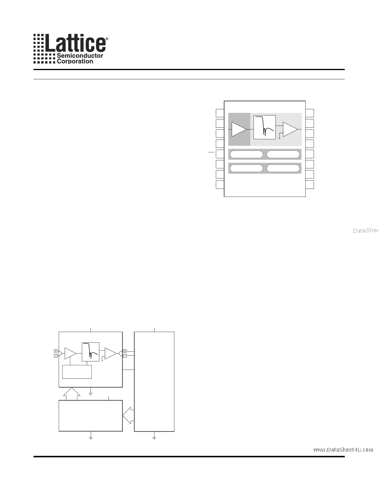
Functional Block Diagram
■ In-System Programmable(ISP™) Analog
• Instrument Amplifier Gain Stage
• Precision Active Filtering (10kHz to 75kHz)
• Continuous-Time Fifth Order Low Pass Topology
• Dual, A/B Configuration Memory
• Non-Volatile E2CMOS® Cells
• IEEE 1149.1 JTAG Serial Port Programming
TMS 1
TCK 2
TDI 3
IA
OA
TDO 4
5th Order LPF
16 VS
15 TEST
14 OUT+
13 OUT–
■ Unique Flexibility and Performance
• Programmable Gain Range (0dB to 20dB)
• Implements Multiple Filter Types: Elliptical,
Chebyshev, Butterworth
• Low Distortion (THD < -80dB at 10kHz)
• Auto-Calibrated Input Offset Voltage
CS 5
CAL 6
ENSPI 7
GND 8
E2CMOS Cfg A E2CMOS Cfg B
Ref & Auto-Cal
ISP Control
12 TEST
11 IN+
10 IN–
9 VREFOUT
■ True Differential I/O
• High CMR Instrument Amplifier Input
ispPAC81
• 2.5V Common Mode Reference on Chip
Description
• Rail-to-Rail Voltage Outputs
■ Single Supply 5V Operation
The ispPAC81 is a member of the Lattice family of In-System
Programmable analog circuits, digitally configured via nonvol-
• Power Dissipation of 133mW
• 16-Pin Plastic SOIC, PDIP Packages
DataSheeta4tUile.cEo2mCMOS technology.
Analog building blocks, called PACell™(s), replace traditional
■ Applications Include Integrated
analog components such as opamps, eliminating the need for
• Single +5V Supply Signal Conditioning
• Programmable Filters With Fully Differential I/O
• Analog Front Ends, 12-Bit Data Acq. Systems
• DSP System Front End Signal Conditioning
• High-Performance Reconstruction Filters
external resistors and capacitors. With no requirement for
external configuration components, ispPAC81 expedites the
design process, simplifying prototype circuit implementation
and change, while providing high-performance integrated
functionality. With all components on chip, there is no longer a
concern of performance degradation due to component mis-
Typical Application Diagram
match or other external factors. The ispPAC81 provides reli-
able and repeatable performance, every time.
5V
ispPAC81
Vin
A/B & Gain
SPI Control
VREFout
5V
5V
12-Bit Differential
Input ADC
Ain+
Ain-
Reference
Designers configure the ispPAC81 and verify its performance
using PAC-Designer®, an easy-to-use, Microsoft Windows®
compatible program. A filter configuration database is pro-
vided whereby thousands of different configurations can be
realized. No special understanding of filter synthesis is
required beyond that of general specifications such as corner
frequency and stopband attenuation, etc. The software lists
the possible choices that meet the designer’s specifications
which can then be loaded directly into either of two device (A/
B) configurations from the lookup table. Device programming
is supported using PC parallel port I/O operations.
The ispPAC81 is configured through its IEEE Standard 1149.1
compliant serial port. The flexible In-System Programming
DSP capability enables programming, verification and reconfigura-
tion, if desired, directly on the printed circuit board.
DataShee
DataSheet4U.com
www.latticesemi.com
DataSheet4 U .com
1 pac81_01
DataSheet4U.com
1 page 
www.DataSheet4U.com
Lattice Semiconductor
Part Number Description
ispPAC81 – XX X X
Device Family
Device Number
ispPAC81 Ordering Information
Part Number
ispPAC81-01PI
ispPAC81-01SI
Package Options
et4U.com
1
DataSheet4U.co1 m
ispPAC81 Data Sheet
Grade
Blank = Commercial
I = Industrial
Package
P = PDIP
S = SOIC
Performance Grade
01 = Standard
Package
16-pin PDIP
16-pin SOIC
DataShee
16-Pin PDIP
16-Pin SOIC
DataSheet4U.com
DataSheet4 U .com
5
DataSheet4U.com
5 Page 
www.DataSheet4U.com
Lattice Semiconductor
ispPAC81 Data Sheet
JTAG User Bits
There are a number of user-configured E2 bits that control various aspects of and can all be accessed in either the
pull-down menus or directly in the schematic design entry screen of the PAC-Designer software interface to the
ispPAC81. See the online help associated with the ispPAC81 in PAC-Designer for more details of how to set/pro-
gram various operation modes. The list of control E2 bits available is listed in Table 3.
Differential I/O
Differential peak-peak voltage is determined by knowing the signal extremes on both differential input or output
pins. For example, if V(+) equals 4V and V(-) equals 1V, the differential voltage is defined as V(+) - V(-) = Vdiff, or
4V - 1V = +3V. Since either polarity can exist on differential I/O pins, it is also possible for the opposite extreme to
exist and would mean when V(+) equals 1V and V(-) equals 4V, the differential voltage is now 1V - 4V = -3V. To cal-
culate the differential peak-peak voltage or full signal swing, the absolute difference between the two extreme
Vdiff’s is calculated. Using the previous examples would result in |(+3V) - (-3V)| = 6V. It can be immediately seen
that true differential signals result in a doubling of usable dynamic range. For more explanation of this and other dif-
ferential circuit benefits, please refer to application note number AN6019, Differential Signaling.
Single-ended Input
To connect the ispPAC81 differential input to a single-ended signal, one of the differential inputs needs to be con-
nected to a DC bias, preferably VREFOUT. The input signal must either be AC coupled or have a DC bias equal to
the DC level of the other input. Since the input voltage is defined as VIN+ - VIN-, the common mode level is ignored.
The signal information is only present on one input, the other being connected to a voltage reference.
et4U.com
Single-ended Output
Connecting the output to a single-ended circuit is simpler still. Simply connect one-half of the differential output, but
not the other. Either output conveys the signal information, just at half the magnitude of the differential output. The
DC level of the single-ended output will be VREFOUT. If the load is not AC coupled and is at a DC potential other
than VREFOUT, the load draws a constant currenDta. tUasSinhgeeotn4eU.ocfotmhe differential outputs halves the available output
voltage swing (3Vp-p versus 6Vp-p). If the load requires DC current, the available voltage swing is reduced. The
output is capable of 10mA, so any DC current raises the minimum allowable load impedance.
DataShee
Input Common-Mode Voltage Range
For the ispPAC81, both maximum input signal range and corresponding common-mode voltage range are a func-
tion of the input gain setting. The maximum input voltage times the gain of an individual PACblock cannot exceed
the output range of that block or clipping will occur. The maximum guaranteed input range is 1V to 4V, with a typical
range of 0.7V to 4.3V for a 5V supply voltage.
The input common-mode voltage is VCM = (VCM+ + VCM-)/2. When the value of VCM is 2.5V, there are no further
input restrictions other than the previously mentioned clipping consideration. This is easily achieved when the input
signal is true differential and referenced to 2.5V.
When VCM is not 2.5V and the gain setting is greater than one, distortion will occur when the maximum input limit is
reached for a particular gain. The lowest VCM for a given gain setting is expressed by the formula, VCM– = 0.675V +
0.584G·VIN where G is the gain setting and VIN is the peak input voltage, expressed as |VIN+ - VIN–| and the highest
VCM is VCM+ = 5.0V - VCM– where 5V is the nominal supply voltage.
In Table 4, the maximum VIN for a given VCM– to VCM+ range is given. If the maximum VIN is known, find the equiv-
alent or greater value under the appropriate gain column and the widest range for VCM will be found horizontally
across in the left-most two columns. Only a VCM range equal to or less than this will give distortion-free perfor-
mance. Conversely, if the maximum VCM range is known, the largest acceptable peak value of VIN can be found in
the corresponding gain column. All values of VIN less than this will give full rated performance.
DataSheet4U.com
DataSheet4 U .com
11
DataSheet4U.com
11 Page | ||
| Páginas | Total 20 Páginas | |
| PDF Descargar | [ Datasheet ISPPAC81.PDF ] | |
Hoja de datos destacado
| Número de pieza | Descripción | Fabricantes |
| ISPPAC80-01PI | In-System Programmable Analog Circuit | Lattice Semiconductor |
| ISPPAC80-01SI | In-System Programmable Analog Circuit | Lattice Semiconductor |
| ISPPAC81 | In-System Programmable Analog Circuit | Lattice Semiconductor |
| Número de pieza | Descripción | Fabricantes |
| SLA6805M | High Voltage 3 phase Motor Driver IC. |
Sanken |
| SDC1742 | 12- and 14-Bit Hybrid Synchro / Resolver-to-Digital Converters. |
Analog Devices |
|
DataSheet.es es una pagina web que funciona como un repositorio de manuales o hoja de datos de muchos de los productos más populares, |
| DataSheet.es | 2020 | Privacy Policy | Contacto | Buscar |