|
|
|
PDF 20N06 Data sheet ( Hoja de datos )
| Número de pieza | 20N06 | |
| Descripción | NTD20N06 | |
| Fabricantes | ETC | |
| Logotipo | ||
Hay una vista previa y un enlace de descarga de 20N06 (archivo pdf) en la parte inferior de esta página. Total 8 Páginas | ||
|
No Preview Available !
www.DataSheet4U.com
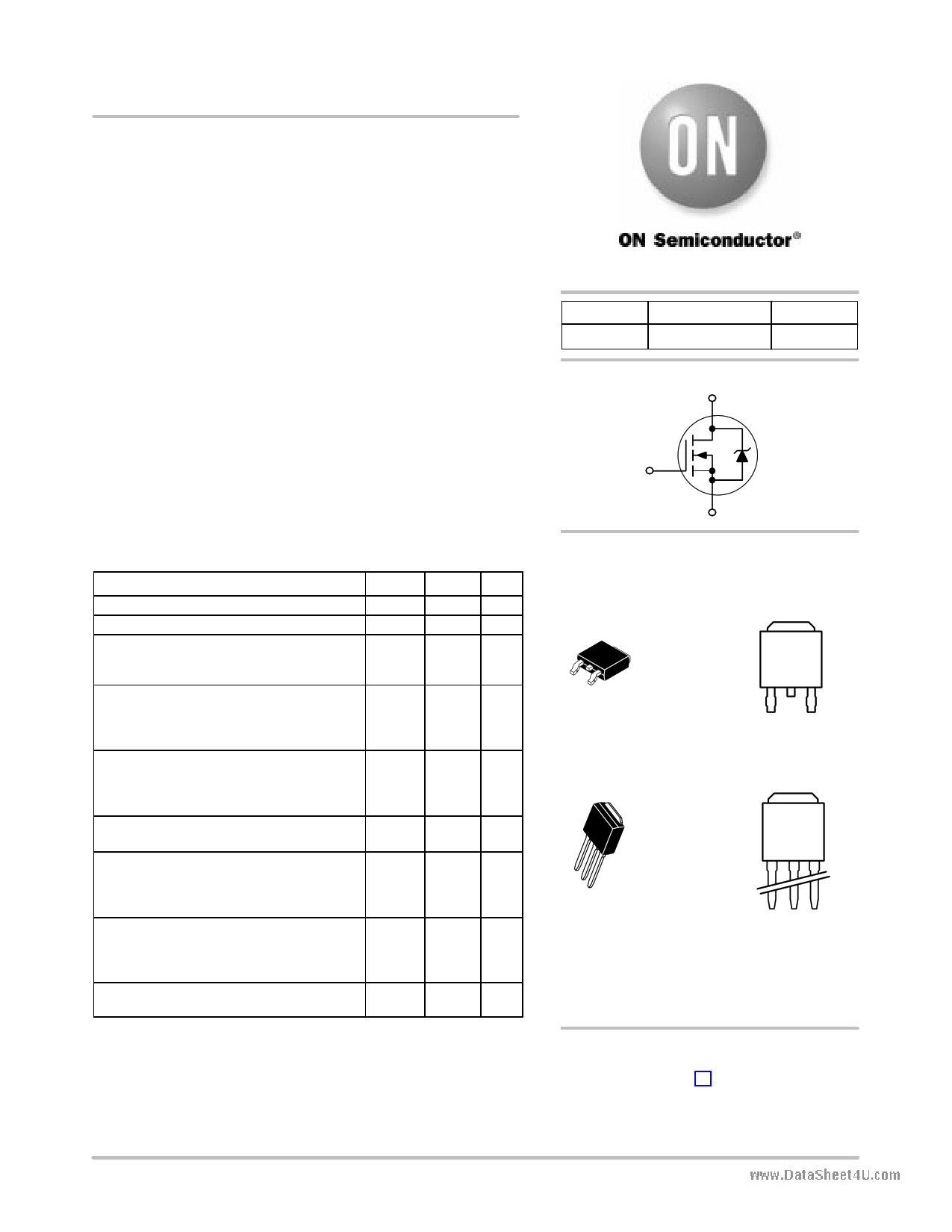
NTD20N06
Power MOSFET
20 Amps, 60 Volts, N−Channel DPAK
Designed for low voltage, high speed switching applications in
power supplies, converters and power motor controls and bridge
circuits.
Features
• Pb−Free Packages are Available
• Lower RDS(on)
• Lower VDS(on)
• Lower Capacitances
• Lower Total Gate Charge
• Lower and Tighter VSD
• Lower Diode Reverse Recovery Time
• Lower Reverse Recovery Stored Charge
Typical Applications
• Power Supplies
• Converters
• Power Motor Controls
• Bridge Circuits
MAXIMUM RATINGS (TJ = 25°C unless otherwise noted)
Rating
Symbol Value Unit
Drain−to−Source Voltage
Drain−to−Gate Voltage (RGS = 10 MW)
Gate−to−Source Voltage
− Continuous
− Non−repetitive (tpv10 ms)
Drain Current
− Continuous @ TA = 25°C
− Continuous @ TA = 100°C
− Single Pulse (tpv10 ms)
Total Power Dissipation @ TA = 25°C
Derate above 25°C
Total Power Dissipation @ TA = 25°C (Note 1)
Total Power Dissipation @ TA = 25°C (Note 2)
Operating and Storage Temperature Range
VDSS
VDGR
VGS
VGS
ID
ID
IDM
PD
TJ, Tstg
60
60
"20
"30
20
10
60
60
0.40
1.88
1.36
−55 to
175
Vdc
Vdc
Vdc
Adc
Apk
W
W/°C
W
W
°C
Single Pulse Drain−to−Source Avalanche
Energy − Starting TJ = 25°C
(VDD = 25 Vdc, VGS = 10 Vdc,
L = 1.0 mH, IL(pk) = 18.4 A, VDS = 60 Vdc)
Thermal Resistance
− Junction−to−Case
− Junction−to−Ambient (Note 1)
− Junction−to−Ambient (Note 2)
Maximum Lead Temperature for Soldering
Purposes, 1/8″ from case for 10 seconds
EAS
RqJC
RqJA
RqJA
TL
170 mJ
°C/W
2.5
80
110
260 °C
Maximum ratings are those values beyond which device damage can occur.
Maximum ratings applied to the device are individual stress limit values (not
normal operating conditions) and are not valid simultaneously. If these limits
are exceeded, device functional operation is not implied, damage may occur
and reliability may be affected.
1. When surface mounted to an FR4 board using the minimum recommended
pad size.
2. When surface mounted to an FR4 board using the 0.5 sq in drain pad size.
© Semiconductor Components Industries, LLC, 2004
August, 2004 − Rev. 6
1
http://onsemi.com
V(BR)DSS
60 V
RDS(on) TYP
37.5 mW
ID MAX
20 A
N−Channel
D
G
S
4
12
3
MARKING
DIAGRAMS
4
Drain
DPAK
CASE 369C
STYLE 2
1
Gate
2
Drain
3
Source
4
1
2
3
DPAK−3
CASE 369D
STYLE 2
4
Drain
12 3
Gate Drain Source
20N06
A
Y
WW
= Device Code
= Assembly Location
= Year
= Work Week
ORDERING INFORMATION
See detailed ordering and shipping information in the package
dimensions section on page 2 of this data sheet.
Publication Order Number:
NTD20N06/D
1 page 
www.DataSheet4U.com
NTD20N06
12
10 QT
8
6 Q1
Q2
VGS
4
2
0
04
ID = 20 A
TJ = 25°C
8 12 16 20 24
QG, TOTAL GATE CHARGE (nC)
Figure 8. Gate−To−Source and Drain−To−Source
Voltage versus Total Charge
1000
VDS = 30 V
ID = 20 A
VGS = 10 V
100
tr
td(off)
10
td(on)
tf
1
1 10
RG, GATE RESISTANCE (OHMS)
Figure 9. Resistive Switching Time
Variation versus Gate Resistance
DRAIN−TO−SOURCE DIODE CHARACTERISTICS
20
VGS = 0 V
16 TJ = 25°C
100
12
8
4
0
0.6 0.7 0.8 0.9
VSD, SOURCE−TO−DRAIN VOLTAGE (VOLTS)
1
Figure 10. Diode Forward Voltage versus Current
SAFE OPERATING AREA
The Forward Biased Safe Operating Area curves define
the maximum simultaneous drain−to−source voltage and
drain current that a transistor can handle safely when it is
forward biased. Curves are based upon maximum peak
junction temperature and a case temperature (TC) of 25°C.
Peak repetitive pulsed power limits are determined by using
the thermal response data in conjunction with the procedures
discussed in AN569, “Transient Thermal Resistance −
General Data and Its Use.”
Switching between the off−state and the on−state may
traverse any load line provided neither rated peak current
(IDM) nor rated voltage (VDSS) is exceeded and the
transition time (tr,tf) do not exceed 10 ms. In addition the total
power averaged over a complete switching cycle must not
exceed (TJ(MAX) − TC)/(RqJC).
A Power MOSFET designated E−FET can be safely used
in switching circuits with unclamped inductive loads. For
reliable operation, the stored energy from circuit inductance
dissipated in the transistor while in avalanche must be less
than the rated limit and adjusted for operating conditions
differing from those specified. Although industry practice is
to rate in terms of energy, avalanche energy capability is not
a constant. The energy rating decreases non−linearly with an
increase of peak current in avalanche and peak junction
temperature.
Although many E−FETs can withstand the stress of
drain−to−source avalanche at currents up to rated pulsed
current (IDM), the energy rating is specified at rated
continuous current (ID), in accordance with industry custom.
The energy rating must be derated for temperature as shown
in the accompanying graph (Figure 12). Maximum energy at
currents below rated continuous ID can safely be assumed to
equal the values indicated.
http://onsemi.com
5
5 Page | ||
| Páginas | Total 8 Páginas | |
| PDF Descargar | [ Datasheet 20N06.PDF ] | |
Hoja de datos destacado
| Número de pieza | Descripción | Fabricantes |
| 20N03HL | MTD20N03HL | Motorola Semiconductors |
| 20N03L | IPD20N03L | Infineon Technologies |
| 20N06 | N-Channel MOSFET Transistor | Inchange Semiconductor |
| 20N06 | NTD20N06 | ETC |
| Número de pieza | Descripción | Fabricantes |
| SLA6805M | High Voltage 3 phase Motor Driver IC. |
Sanken |
| SDC1742 | 12- and 14-Bit Hybrid Synchro / Resolver-to-Digital Converters. |
Analog Devices |
|
DataSheet.es es una pagina web que funciona como un repositorio de manuales o hoja de datos de muchos de los productos más populares, |
| DataSheet.es | 2020 | Privacy Policy | Contacto | Buscar |