|
|
PDF NTTS2P02R2 Data sheet ( Hoja de datos )
| Número de pieza | NTTS2P02R2 | |
| Descripción | Power MOSFET ( Transistor ) | |
| Fabricantes | ON Semiconductor | |
| Logotipo | ||
Hay una vista previa y un enlace de descarga de NTTS2P02R2 (archivo pdf) en la parte inferior de esta página. Total 8 Páginas | ||
|
No Preview Available !
www.DataSheet4U.com
NTTS2P02R2
Power MOSFET
-2.4 Amps, -20 Volts
Single P–Channel Micro8t
Features
• Ultra Low RDS(on)
• Higher Efficiency Extending Battery Life
• Logic Level Gate Drive
• Miniature Micro–8 Surface Mount Package
• Diode Exhibits High Speed, Soft Recovery
• Micro8 Mounting Information Provided
Applications
• Power Management in Portable and Battery–Powered Products, i.e.:
Cellular and Cordless Telephones and PCMCIA Cards
MAXIMUM RATINGS (TJ = 25°C unless otherwise noted)
Rating
Symbol Value Unit
Drain–to–Source Voltage
Gate–to–Source Voltage – Continuous
Thermal Resistance –
Junction–to–Ambient (Note 1.)
Total Power Dissipation @ TA = 25°C
Continuous Drain Current @ TA = 25°C
Continuous Drain Current @ TA = 70°C
Pulsed Drain Current (Note 3.)
Thermal Resistance –
Junction–to–Ambient (Note 2.)
Total Power Dissipation @ TA = 25°C
Continuous Drain Current @ TA = 25°C
Continuous Drain Current @ TA = 70°C
Pulsed Drain Current (Note 3.)
Operating and Storage
Temperature Range
VDSS
VGS
–20
±8.0
V
V
RθJA
PD
ID
ID
IDM
160 °C/W
0.78 W
–2.4 A
–1.92
A
Da–ta20Sheet4AU.com
RθJA
PD
ID
ID
IDM
TJ, Tstg
88
1.42
–3.25
–2.6
–30
–55 to
+150
°C/W
W
A
A
A
°C
Single Pulse Drain–to–Source Avalanche
Energy – Starting TJ = 25°C
(VDD = –20 Vdc, VGS = –4.5 Vdc,
Peak IL = –5.0 Apk, L = 28 mH,
RG = 25 Ω)
Maximum Lead Temperature for Soldering
Purposes for 10 seconds
EAS
TL
350 mJ
260 °C
1. Minimum FR–4 or G–10 PCB, Steady State.
2. Mounted onto a 2″ square FR–4 Board (1″ sq. 2 oz Cu 0.06″ thick single
sided), Steady State.
3. Pulse Test: Pulse Width ≤ 300 ms, Duty Cycle ≤ 2%.
http://onsemi.com
–2.4 AMPERES
–20 VOLTS
RDS(on) = 90 mW
Single P–Channel
D
G
8
1
Micro8
CASE 846A
STYLE 1
S
MARKING
DIAGRAM
YWW
AD
Y = Year
WW = Work Week
AD = Device Code
PIN ASSIGNMENT
Source
Source
Source
Gate
18
27
36
45
Top View
Drain
Drain
Drain
Drain
ORDERING INFORMATION
Device
Package
Shipping
NTTS2P02R2 Micro8 4000/Tape & Reel
DataShee
DataSheet4U.com
© Semiconductor Components Industries, LLC, 2000
December, 2000 – Rev. 4
1
Publication Order Number:
NTTS2P02R2/D
1 page 
www.DataSheet4U.com
1
NTTS2P02R2
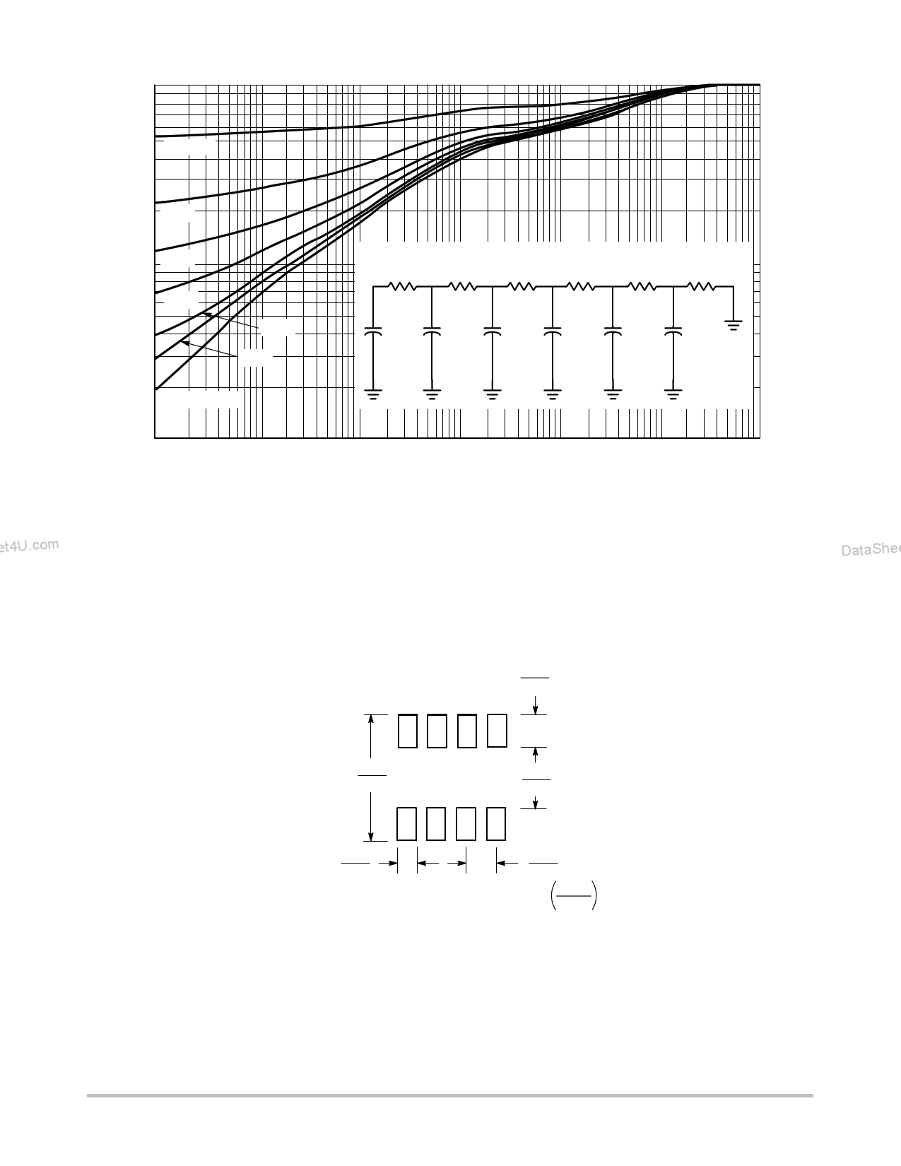
D = 0.5
0.2
0.1 0.1
0.05
0.02
0.01
Normalized to R∅ja at Steady State (1 inch pad)
0.0125 Ω 0.0563 Ω 0.110 Ω 0.273 Ω 0.113 Ω 0.436 Ω
0.021 F 0.137 F 1.15 F 2.93 F 152 F
261 F
Single Pulse
0.01
1E–03
1E–02
1E–01
1E+00
t, TIME (s)
1E+03
Figure 13. FET Thermal Response.
1E+02
1E+03
et4U.com
INFORMATION FOR USING THE Micro–8 SURFACE MOUNT PACKAGE
MINIMUM RECOMMENDED FOOTDPaRtaINSTheFeOt4RUS.cUoRmFACE MOUNTED APPLICATIONS
Surface mount board layout is a critical portion of the total
design. The footprint for the semiconductor packages must
be the correct size to ensure proper solder connection
interface between the board and the package. With the
correct pad geometry, the packages will self–align when
subjected to a solder reflow process.
0.041
1.04
DataShee
0.208
5.28
0.015
0.38
0.126
3.20
0.0256
0.65
inches
mm
DataSheet4U.com
http://onsemi.com
5
5 Page | ||
| Páginas | Total 8 Páginas | |
| PDF Descargar | [ Datasheet NTTS2P02R2.PDF ] | |
Hoja de datos destacado
| Número de pieza | Descripción | Fabricantes |
| NTTS2P02R2 | Power MOSFET ( Transistor ) | ON Semiconductor |
| Número de pieza | Descripción | Fabricantes |
| SLA6805M | High Voltage 3 phase Motor Driver IC. |
Sanken |
| SDC1742 | 12- and 14-Bit Hybrid Synchro / Resolver-to-Digital Converters. |
Analog Devices |
|
DataSheet.es es una pagina web que funciona como un repositorio de manuales o hoja de datos de muchos de los productos más populares, |
| DataSheet.es | 2020 | Privacy Policy | Contacto | Buscar |
