|
|
|
PDF LX1994 Data sheet ( Hoja de datos )
| Número de pieza | LX1994 | |
| Descripción | High Efficiency LED Driver | |
| Fabricantes | Microsemi Corporation | |
| Logotipo | ||
Hay una vista previa y un enlace de descarga de LX1994 (archivo pdf) en la parte inferior de esta página. Total 13 Páginas | ||
|
No Preview Available !
www.DataSheet4U.com
LX1994
TM ® High Efficiency LED Driver
PRODUCTION DATA SHEET
DESCRIPTION
Microsemi’s LX1994 is a compact, The use of external N-channel
high efficiency, step-up boost MOSFET allows design to optimize
controller which is designed to drive a system efficiency.
string of white or colored LED’s in a The OVP protection comparator
backlight or front light system. The eliminates the need of an external Zener
LX1994 design is based on a dual diode clamp. The OVP function can be
mode PFM architecture and provides scaled for any output voltage.
maximum typical efficiency greater Maximum output current is achievable
than 92%.
by selection of the current sense
The LX1994 has many unique resistor. These features make the
design features and advantages over controller ideal for PDA or digital
competitor solutions. The features camera applications
included: low quiescent current To enhance system battery life, the
(100µA typical), low shut down LX1994 provides 2 dimming options
current (<1µA), dedicate ambient light and a dedicated ambient light sensor
sensor interface (LX1970), dual (LX1970) interface.
dimming modes, low voltage and low The LX1994 supports a wide range
offset current sense, and integrated of system battery voltage inputs which
OVP protection.
ranges from 2.0 to 5.5V. The LX1994
The converter achieves high is guaranteed to start up at 2.0V input.
efficiency, low cost, and flexible The LX1994 is available in miniature
design by selection of an external N- 10-pin MLP or MSOP packages.
Channel MOSFET, current sense
resistors, and integrated OVP
protection.
IMPORTANT: For the most current data, consult MICROSEMI’s website: http://www.microsemi.com
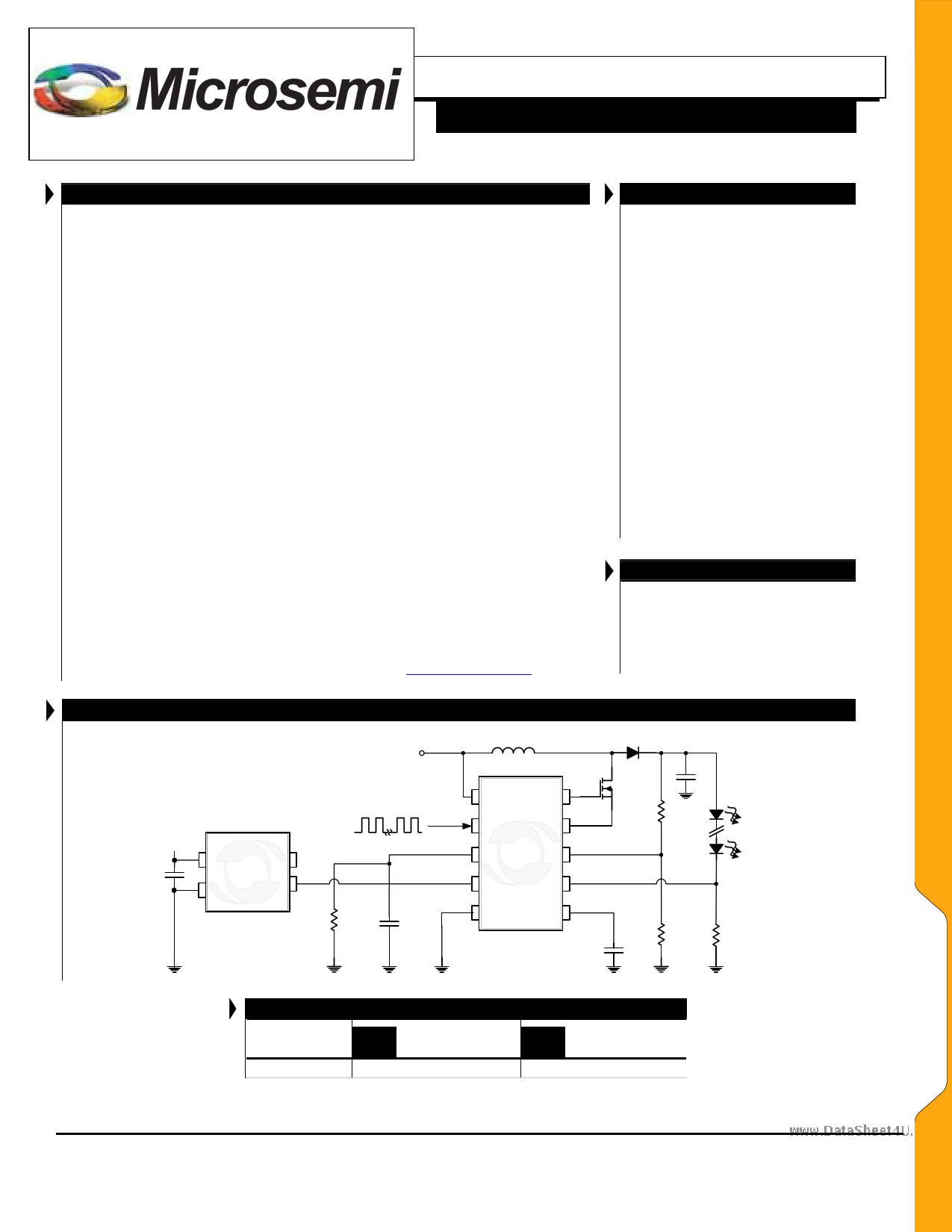
Auto Adjust for
Ambient Light
3V
VDD
SNK
VSS
SRC
LX1970
PRODUCT HIGHLIGHT
VIN = 2.0V to 5.5V
33µH
LX1994
VIN DRV
S/P SRC
BRT
OVP
LS FB
GND
CMP
KEY FEATURES
Efficiency > 92%
Dual PFM Architecture To
Extend Battery Life
VIN Range 2.0V To 5.5V. Start
Up Warranty @ 2.0V
Logic Control Shutdown
100µA Typical Quiescent
Current
Shutdown IQ Current <1µA
OVP For Open String Output
Voltage
Low Voltage And Offset
Current Sense
Light Sensor (LX1970)
interface
Dual Dimming Options (PWM
or DC Voltage)
No External Zener Clamp
Diode
10-Pin MLP or MSOP
APPLICATIONS
Pagers
PDA
Cell Phone
Portable Display
Digital Cameras
UPS5819
FDV303
Copyright © 2003
Rev. 1.0a, 2004-08-10
DataSheet4 U .com
TA (°C)
-40 to 85
PACKAGE ORDER INFO
Plastic MLP
Plastic MSOP
LD 10-Pin
DU 10-Pin
LX1994CLD
LX1994CDU
Note: Available in Tape & Reel. Append the letters “TR” to the part number. (i.e.
LX1994CDU-TR)
Microsemi
Integrated Products Division
11861 Western Avenue, Garden Grove, CA. 92841, 714-898-8121, Fax: 714-893-2570
Page 1
1 page 
www.DataSheet4U.com
LX1994
TM ® High Efficiency LED Driver
PRODUCTION DATA SHEET
THEORY OF OPERATION
Basic PFM operation
The LX1994 dual mode PFM modulator is implemented in
two switching modes: the hysteretic and Continuous
Switching Mode (CSM).
In hysteretic switching mode, the basic PFM modulator
logic/timing block uses a Fixed Peak Current/ Fixed Off
Time where the switch turns on and allows the inductor
current to ramp to a finite peak level then shuts off for a
fixed duration of time. The basic modulation cycle repeats
as long as the converter output voltage is less than the
maximum regulation level. When the maximum regulation
level is reached, the switch remains off until the output
voltage capacitor discharges to a level less than the
minimum regulation level. The input signals to the switch
logic block are the burst on/off control signal and the peak
current detection signals. For low and negligible switch
conduction losses the designer may set the peak current
comparator at 20mV corresponding to 200mA of output
current.
In Continuous Switching Mode (CSM), the level to the
peak current comparator is variable. This current level is
developed by integrating the output of the feedback
comparator which functions as a high gain bandwidth
limited error amplifier. This current is clamped to the peak
switch current limit of 600mA. The integrated capacitor is
attached at the CMP pin when the burst on/off control line
is forced to the “ON” state.
The conversion from hysteretic to CSM mode is performed
when the burst length exceeds more than 16 switching
cycles counting by an internal 16 bits shift register. The
internal register is clocked by the switch transitions during
each burst period. When the switching cycles exceed 16
cycles, the converter automatically switches over to CSM
mode. CSM mode switching is latched by a J/K flip-flop.
The conversion from CSM mode to hysteretic mode is
performed when the error amplifier output falls below
10mV (corresponding to 100mA peak current) as
determined by a comparator. This resets the J/K flip-flop
and converts back to hysteric mode.
The LX1994 is a highly efficient PFM boost converter, its
design is based on dual mode PFM for driving a series of
white or color LEDs. The advantage of PFM switching is
to minimize system efficiency losses in both heavy and
light load operations. The LX1994 does not require an
external oscillator due to PFM dual modes switching.
In light load operation, the converter minimizes switching
losses by delivering more energy than necessary during
switching burst period than the inactivity coast period.
In heavy load condition, the converter uses the
Continuous Switching Current Mode (CSM) regulation
scheme. This minimized peak switching current and
thereby minimizes the conduction losses.
Losses
There are two types of losses in PFM regulator design: the
switching loss, and conduction loss; that contribute to
system inefficiency.
Switching loss: Energy switching losses are associated
with a NFET’s switch changing state (from on to off or
vice versa) as a simultaneous high level of voltage and
current are at the NFET’s switch during the transition.
This switching loss is proportional to the switching
frequency.
Conduction loss: the loss due to current flow in the series
resistance of the switch, inductor, and current sense
resistor. Conduction loss is proportional to the square of
the switch current.
Output Current Selection
The LED output current is regulated by adjusting of the
FB pin voltage. If the FB pin voltage equals the BRT pin
voltage, the LED current is the result of the FB pin
voltage divided by the selected current sense resistor.
For example: in a 100% duty cycle design, FB pin voltage
is 300mV, the current sense resistor is 15Ω. The LED
current equals:
300mV
= 20mA
15Ω
Copyright © 2003
Rev. 1.0a, 2004-08-10
DataSheet4 U .com
Microsemi
Integrated Products Division
11861 Western Avenue, Garden Grove, CA. 92841, 714-898-8121, Fax: 714-893-2570
Page 5
5 Page 
www.DataSheet4U.com
LX1994
TM ® High Efficiency LED Driver
PRODUCTION DATA SHEET
APPLICATION INFORMATION
R3 = 23.2k
The level at 100% duty cycle in full darkness is 4mA,
which is 20% of the maximum level of 20mA; this implies
80% is attributable to ISCR. Combining this information with
the describing equation for AUTO mode gives:
( ) (( ) ( ) )80%×ILED(MAX)×R5=
ISRC × R1×R2×Rp
R1×R2 + R1×Rp + R2×Rp
This implies:
( R1×R2×Rp )
0.8×.02×15
( ) ( ) ( ) = =2.4k
R1×R2 + R1×Rp + R2×Rp
100µA
Since the left side is the three resistors in parallel, this can
be restated as:
416×10-6 = 1 + 1 + 1 =G1+G2+Gp
R1 R2 Rp
The manual mode equation can be reduced to this assuming
100% duty and 20mA LED current (that is 0.3V sense
resistor voltage):
R2×Rp
=
0.3×R1
0.3×R1
=
R2+Rp (10µA×R1)+VCC -0.3 (10µA×R1)+3.0
This can be restated as:
( )1 + 1 =33×10-6 + 10 or G2+Gp=33×10-6 + 10×G1
R2 Rp
R1
The auto mode equation can be reduced to this assuming
100% duty , 100µA ISRC current and 20mA LED current
(that is 0.3V sense resistor voltage):
R1×Rp
0.3×R2
( )=
R1+Rp (ISRC +10µA)×R2 +VCC -0.3
0.3×R2
0.3×R2
==
( ) ( )(100µ+10µA)×R2 +VCC -0.3 110µA×R2 +3.0
This can be restated as:
( )1 + 1 =367×10-6 + 10 or G1+Gp=367×10-6 + 10×G2
R1 Rp
R2
The equations above can be solved for G1, G2 and Gp:
G1=34.8×10⁻⁶
G2=4.45×10⁻⁶
Gp=376×10-6
Knowing Gp we can find
G4=Gp- 1 =343×10-6
30k
The resistance values are the reciprocal of the
conductance’s so:
R1 = 28.7k
R2 = 225k
R4 = 2.91k
The value of C1 is selected to give a time constant of ½
second and works into R3 (which is 23.2k).
0.5
C1=
C1 = 21.5µF
23.2k
The value of C2 works into Rp and the pole should be set
at 1/100 of the PWM frequency.
1
C2=
10kHz
6.28×
×2.66k
100
For a 10KHz PWM, C2 = 599nF, and a value of 1µf
works well.
Circuit of Figure 3:
The second light sensor interface is very similar to the first;
the choice is a matter of user preference. In the second
circuit, an active 325mV clamp is used to clamp the
maximum LED current in auto mode.
In this circuit, resistor R3 is reduced to extend the
operating ambient light range of the light sensor and filter
capacitor C1 must therefore be increased.
Copyright © 2003
Rev. 1.0a, 2004-08-10
DataSheet4 U .com
Microsemi
Integrated Products Division
11861 Western Avenue, Garden Grove, CA. 92841, 714-898-8121, Fax: 714-893-2570
Page 11
11 Page | ||
| Páginas | Total 13 Páginas | |
| PDF Descargar | [ Datasheet LX1994.PDF ] | |
Hoja de datos destacado
| Número de pieza | Descripción | Fabricantes |
| LX1990 | Dual Programmable LED Current Sink | Microsemi Corporation |
| LX1991 | Six Output Programmable LED Current Sink | Microsemi Corporation |
| LX1993 | High Efficiency LED Driver | Microsemi Corporation |
| LX1994 | High Efficiency LED Driver | Microsemi Corporation |
| Número de pieza | Descripción | Fabricantes |
| SLA6805M | High Voltage 3 phase Motor Driver IC. |
Sanken |
| SDC1742 | 12- and 14-Bit Hybrid Synchro / Resolver-to-Digital Converters. |
Analog Devices |
|
DataSheet.es es una pagina web que funciona como un repositorio de manuales o hoja de datos de muchos de los productos más populares, |
| DataSheet.es | 2020 | Privacy Policy | Contacto | Buscar |