|
|
|
PDF AD9411 Data sheet ( Hoja de datos )
| Número de pieza | AD9411 | |
| Descripción | 170/200 MSPS 3.3 V A/D Converter | |
| Fabricantes | Analog Devices | |
| Logotipo | ||
Hay una vista previa y un enlace de descarga de AD9411 (archivo pdf) en la parte inferior de esta página. Total 28 Páginas | ||
|
No Preview Available !
Data Sheet
FEATURES
SNR = 60 dB @ fIN up to 70 MHz @ 200 MSPS
ENOB of 9.8 @ fIN up to 70 MHz @ 200 MSPS (–0.5 dBFS)
SFDR = 80 dBc @ fIN up to 70 MHz @ 200 MSPS (–0.5 dBFS)
Excellent linearity:
DNL = ±0.15 LSB (typical)
INL = ±0.25 LSB (typical)
LVDS output levels
700 MHz full-power analog bandwidth
On-chip reference and track-and-hold
Power dissipation = 1.25 W typical @ 200 MSPS
1.5 V input voltage range
3.3 V supply operation
Output data format option
Clock duty cycle stabilizer
Pin compatible to LVDS mode AD9430
APPLICATIONS
Wireless and wired broadband communications
Cable reverse path
Communications test equipment
Radar and satellite subsystems
Power amplifier linearization
GENERAL DESCRIPTION
The AD9411 is a 10-bit monolithic sampling analog-to-digital
converter optimized for high performance, low power, and ease
of use. The product operates up to a 200 MSPS conversion rate
and is optimized for outstanding dynamic performance in
wideband carrier and broadband systems. All necessary
functions, including track-and-hold (T/H) and reference, are
included on the chip to provide a complete conversion solution.
The ADC requires a 3.3 V power supply and a differential
sample clock for full performance operation. The digital outputs
are LVDS compatible and support both twos complement and
offset binary format. A data clock output is available to ease
data capture.
Fabricated on an advanced BiCMOS process, the AD9411 is
available in a 100-lead surface-mount plastic package (e-PAD
TQFP-100) specified over the industrial temperature range
(–40°C to +85°C).
Rev. B
Information furnished by Analog Devices is believed to be accurate and reliable. However, no
responsibility is assumed by Analog Devices for its use, nor for any infringements of patents or other
rights of third parties that may result from its use. Specifications subject to change without notice. No
license is granted by implication or otherwise under any patent or patent rights of Analog Devices.
Trademarksandregisteredtrademarksarethepropertyoftheirrespectiveowners.
10-Bit, 170/200 MSPS
3.3 V A/D Converter
AD9411
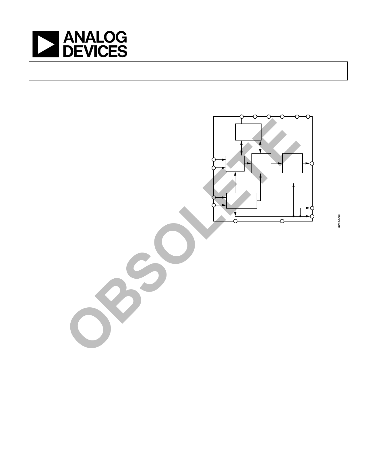
FUNCTIONAL BLOCK DIAGRAM
SENSE VREF AGND DRGND DRVDD AVDD
SCALABLE
REFERENCE
AD9411
VIN+
VIN–
TRACK
AND
HOLD
ADC
10-BIT
PIPELINE
10
/
CORE
LVDS
OUTPUTS
DATA,
OVERRANGE
IN LVDS
CLK+
CLK–
CLOCK
MANAGEMENT
LVDS TIMING
S1 S5
Figure 1.
DCO+
DCO–
PRODUCT HIGHLIGHTS
1. High performance.
Maintains 60 dB SNR @ 200 MSPS with a 70 MHz input.
2. Low power.
Consumes only 1.25 W @ 200 MSPS.
3. Ease of use.
LVDS output data and output clock signal allow interface
to current FPGA technology. The on-chip reference and
sample-and-hold function provide flexibility in system
design. Use of a single 3.3 V supply simplifies system
power supply design.
4. Out-of-range (OR).
The OR output bit indicates when the input signal is
beyond the selected input range.
One Technology Way, P.O. Box 9106, Norwood, MA 02062-9106, U.S.A.
Tel: 781.329.4700
www.analog.com
Fax: 781.461.3113 ©2004–2012 Analog Devices, Inc. All rights reserved.
1 page 
Data Sheet
AD9411
DIGITAL SPECIFICATIONS
AVDD = 3.3 V, DRVDD = 3.3 V, TMIN = –40°C, TMAX = +85°C, unless otherwise noted.
Table 3.
Parameter
CLOCK INPUTS
(CLK+, CLK–)1
Differential Input Voltage2
Common-Mode Voltage3
Input Resistance
Input Capacitance
LOGIC INPUTS (S1, S2, S4, S5)
Logic 1 Voltage
Logic 0 Voltage
Logic 1 Input Current
Logic 0 Input Current
Input Resistance
Input Capacitance
LVDS LOGIC OUTPUTS4
VOD Differential Output Voltage
VOS Output Offset Voltage
Output Coding
AD9411-170
Temp Test Level Min
Typ Max
Full IV
Full VI
Full VI
25°C V
Full IV
Full IV
Full VI
Full VI
25°C V
25°C V
Full VI
Full VI
0.2
1.375
3.2
1.5 1.575
5.5 6.5
4
2.0
0.8
190
10
30
4
247 454
1.125
1.375
Twos Complement or Binary
AD9411-200
Min Typ
Max
0.2
1.375
3.2
1.5
5.5
4
1.575
6.5
2.0
30
4
0.8
190
10
247 454
1.125
1.375
Twos Complement or Binary
Unit
V
V
kΩ
pF
V
V
μA
μA
kΩ
pF
mV
V
1 See the Equivalent Circuits section.
2 All ac specifications tested by driving CLK+ and CLK– differentially, |(CLK+) – (CLK–)| > 200 mV.
3 Clock inputs’ common mode can be externally set, such that 0.9 V < CLK< 2.6 V.
4 LVDS RTERM = 100 Ω, LVDS output current set resistor (RSET) = 3.74 kΩ(1% tolerance).
Rev. B | Page 5 of 28
5 Page 
Data Sheet
Noise (for Any Range within the ADC)
Calculated as follows:
VNOISE
Z
0.00110 FSdBM
SNRdBc
10
SignaldBFS
where Z is the input impedance, FS is the full scale of the device
for the frequency in question, SNR is the value of the particular
input level, and Signal is the signal level within the ADC reported
in dB below full scale. This value includes both thermal and
quantization noise.
Power Supply Rejection Ratio (PSRR)
The ratio of a change in input offset voltage to a change in
power supply voltage.
Signal-to-Noise-and-Distortion (SINAD)
The ratio of the rms signal amplitude (set 1 dB below full scale)
to the rms value of the sum of all other spectral components,
including harmonics but excluding dc.
Signal-to-Noise Ratio (without Harmonics)
The ratio of the rms signal amplitude (set at 1 dB below full
scale) to the rms value of the sum of all other spectral compo-
nents, excluding the first five harmonics and dc.
Spurious-Free Dynamic Range (SFDR)
The ratio of the rms signal amplitude to the rms value of the
peak spurious spectral component. The peak spurious compo-
nent may or may not be a harmonic. May be reported in dBc
(i.e., degrades as signal level is lowered) or dBFS (always related
back to converter full scale).
AD9411
Two-Tone Intermodulation Distortion Rejection
The ratio of the rms value of either input tone to the rms value of
the worst third-order intermodulation product, reported in dBc.
Two-Tone SFDR
The ratio of the rms value of either input tone to the rms value
of the peak spurious component. The peak spurious component
may or may not be an IMD product. May be reported in dBc
(i.e., degrades as signal level is lowered) or in dBFS (always
related back to converter full scale).
Worst Other Spur
The ratio of the rms signal amplitude to the rms value of the
worst spurious component (excluding the second and third
harmonics) reported in dBc.
Transient Response Time
The time it takes for the ADC to reacquire the analog input
after a transient from 10% above negative full scale to 10%
below positive full scale.
Out-of-Range Recovery Time
The time it takes for the ADC to reacquire the analog input
after a transient from 10% above positive full scale to 10% above
negative full scale, or from 10% below negative full scale to 10%
below positive full scale.
Rev. B | Page 11 of 28
11 Page | ||
| Páginas | Total 28 Páginas | |
| PDF Descargar | [ Datasheet AD9411.PDF ] | |
Hoja de datos destacado
| Número de pieza | Descripción | Fabricantes |
| AD9410 | 210 MSPS ADC | Analog Devices |
| AD9411 | 170/200 MSPS 3.3 V A/D Converter | Analog Devices |
| Número de pieza | Descripción | Fabricantes |
| SLA6805M | High Voltage 3 phase Motor Driver IC. |
Sanken |
| SDC1742 | 12- and 14-Bit Hybrid Synchro / Resolver-to-Digital Converters. |
Analog Devices |
|
DataSheet.es es una pagina web que funciona como un repositorio de manuales o hoja de datos de muchos de los productos más populares, |
| DataSheet.es | 2020 | Privacy Policy | Contacto | Buscar |