|
|
|
PDF WF4M16-XDTX5 Data sheet ( Hoja de datos )
| Número de pieza | WF4M16-XDTX5 | |
| Descripción | 2x2Mx16 5V FLASH MODULE | |
| Fabricantes | White Electronic | |
| Logotipo | ||
Hay una vista previa y un enlace de descarga de WF4M16-XDTX5 (archivo pdf) en la parte inferior de esta página. Total 11 Páginas | ||
|
No Preview Available !
www.DataSheet4U.com
WF4M16-XDTX5
HI-RELIABILITY PRODUCT
2x2Mx16 5V FLASH MODULE ADVANCED*
FEATURES
s Access Time of 90, 120, 150ns
s Packaging:
• 56 Lead, Hermetic Ceramic, 0.520" CSOP (Package 213).
Fits standard 56 SSOP footprint.
s Sector Architecture
• 32 equal size sectors of 64KBytes per each 2Mx8 chip
• Any combination of sectors can be erased. Also supports
full chip erase.
s Minimum 100,000 Write/Erase Cycles Minimum
s Organized as two banks of 2Mx16; User Configurable as
4 x 2Mx8
s Commercial, Industrial, and Military Temperature Ranges
s 5 Volt Read and Write. 5V ± 10% Supply.
s Low Power CMOS
s Data Polling and Toggle Bit feature for detection of program
or erase cycle completion.
s Supports reading or programming data to a sector not being
erased.
s Built-in Decoupling Caps and Multiple Ground Pins for Low
Noise Operation, Separate Power and Ground Planes to
improve noise immunity
s RESET pin resets internal state machine to the read mode.
s Ready/Busy (RY/BY) output for direction of program or erase
cycle completion.
* This data sheet describes a product that may or may not be under
development and is subject to change or cancellation without notice.
Note: For programming information refer to Flash Programming 16M5
Application Note.
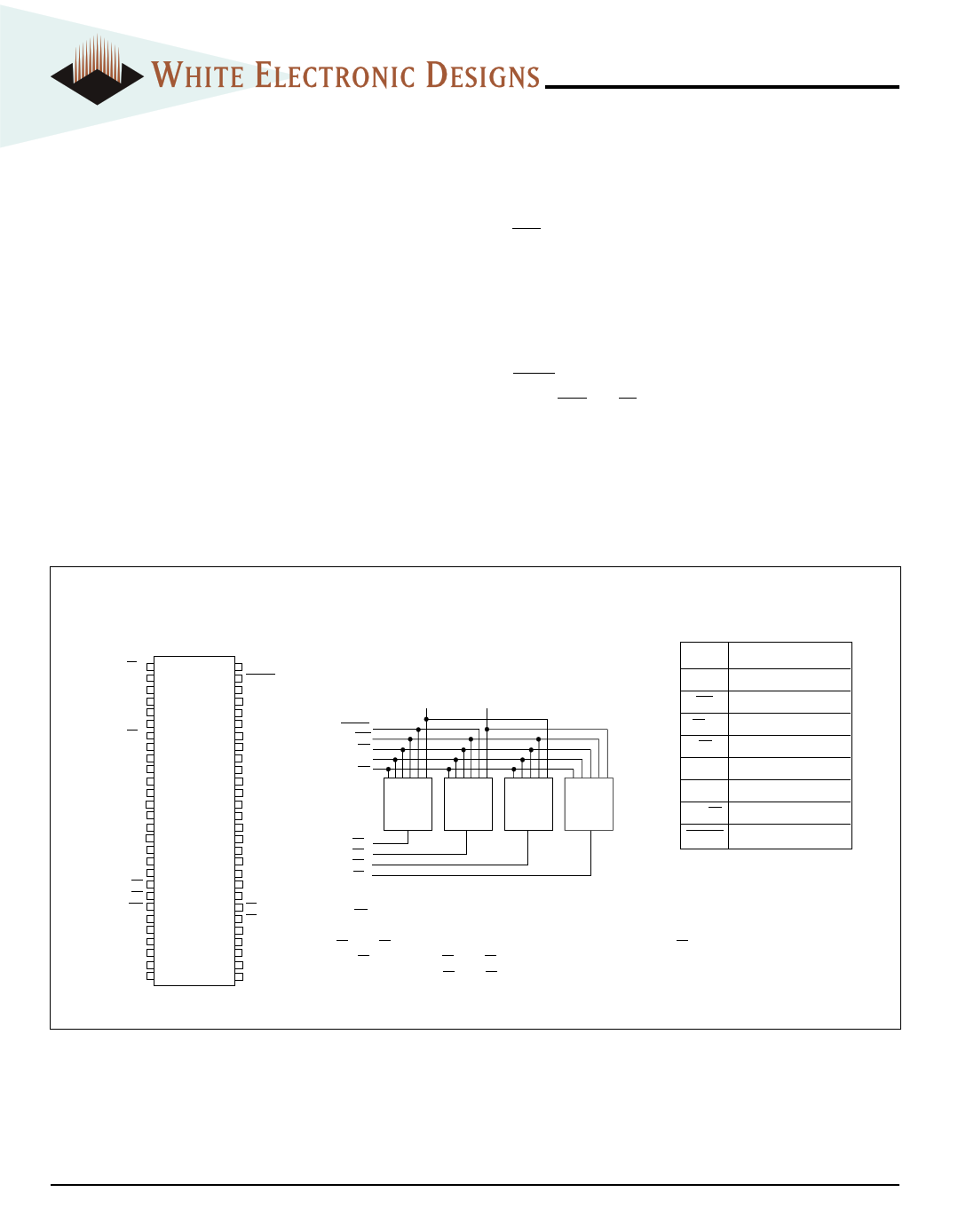
FIG. 1 PIN CONFIGURATION FOR WF4M16-XDTX5
56 CSOP
TOP VIEW
CS1
A12
A13
A14
A15
NC
CS2
NC
A20
A19
A18
A17
A16
VCC
GND
I/O6
I/O14
I/O7
I/O15
RY/BY
OE
WE
NC
I/O13
I/O5
I/O12
I/O4
VCC
1
2
3
4
5
6
7
8
9
10
11
12
13
14
15
16
17
18
19
20
21
22
23
24
25
26
27
28
56 NC
55 RESET
54 A11
53 A10
52 A9
51 A1
50 A2
49 A3
48 A4
47 A5
46 A6
45 A7
44 GND
43 A8
42 VCC
41 I/O9
40 I/O1
39 I/O8
38 I/O0
37 A0
36 NC
35 CS3
34 CS4
33 I/O2
32 I/O10
31 I/O3
30 I/O11
29 GND
PIN DESCRIPTION
BLOCK DIAGRAM
I/O0-15 Data Inputs/Outputs
A0-20
Address Inputs
I/O0-7
I/O8-15
WE Write Enable
RESET
WE
OE
A0-20
RY/BY
CS1-4
OE
VCC
Chip Selects
Output Enable
Power Supply
2M x 8
2M x 8
2M x 8
2M x 8
GND
RY/BY
Ground
Ready/Busy
CS1
RESET
Reset
CS2
CS3
CS4
NOTE:
1. RY/BY is an open drain output and should be pulled-up to Vcc with an
external resistor.
2. CS1 and CS3 control the same data bus. Reads cannot be done with CS1
and CS3 both active. CS2 and CS4 control the same data bus. Reads
cannot be done with CS2 and CS4 both active.
3. Address compatible with Intel 2M8 56 SSOP.
November 1999 Rev.3
1 White Electronic Designs Corporation • (602) 437-1520 • www.whiteedc.com
1 page 
FIG. 3
AC WAVEFORMS FOR READ OPERATIONS
WF4M16-XDTX5
5 White Electronic Designs Corporation • (602) 437-1520 • www.whiteedc.com
5 Page 
WF4M16-XDTX5
ORDERING INFORMATION
W F 4M16 - XXX DT X 5 X
LEAD FINISH:
Blank = Gold plated leads
A = Solder dip leads
VPP PROGRAMMING VOLTAGE
5=5V
DEVICE GRADE:
M = Military, 883 Screened -55°C to +125°C
I = Industrial
-40°C to +85°C
C = Commercial
0°C to +70°C
PACKAGE TYPE:
DT = 56 Lead Dual Cavity CSOP (Package 213)
fits standard 56 SSOP footprint
ACCESS TIME (ns)
ORGANIZATION, 2M x 16
User configurable as 4 x 2M x 8
Flash
WHITE ELECTRONIC DESIGNS CORP.
11 White Electronic Designs Corporation • (602) 437-1520 • www.whiteedc.com
11 Page | ||
| Páginas | Total 11 Páginas | |
| PDF Descargar | [ Datasheet WF4M16-XDTX5.PDF ] | |
Hoja de datos destacado
| Número de pieza | Descripción | Fabricantes |
| WF4M16-XDTX5 | 2x2Mx16 5V FLASH MODULE | White Electronic |
| Número de pieza | Descripción | Fabricantes |
| SLA6805M | High Voltage 3 phase Motor Driver IC. |
Sanken |
| SDC1742 | 12- and 14-Bit Hybrid Synchro / Resolver-to-Digital Converters. |
Analog Devices |
|
DataSheet.es es una pagina web que funciona como un repositorio de manuales o hoja de datos de muchos de los productos más populares, |
| DataSheet.es | 2020 | Privacy Policy | Contacto | Buscar |