|
|
|
PDF AD7951 Data sheet ( Hoja de datos )
| Número de pieza | AD7951 | |
| Descripción | 14-Bit Programmable Input ADC | |
| Fabricantes | Analog Devices | |
| Logotipo | ||
Hay una vista previa y un enlace de descarga de AD7951 (archivo pdf) en la parte inferior de esta página. Total 30 Páginas | ||
|
No Preview Available !
www.DataSheet4U.com
14-Bit, 1 MSPS, Unipolar/Bipolar
Programmable Input PulSAR® ADC
AD7951
FEATURES
Multiple pins/software programmable input ranges:
5 V, 10 V, ±5 V, ±10 V
Pins or serial SPI® compatible input ranges/mode selection
Throughput
1 MSPS (warp mode)
800 kSPS (normal mode)
670 kSPS (impulse mode)
14-bit resolution with no missing codes
INL: ±0.3 LSB typ, ±1 LSB max (±61 ppm of FSR)
SNR: 85 dB @ 2 kHz
iCMOS® process technology
5 V internal reference: typical drift 3 ppm/°C; TEMP output
No pipeline delay (SAR architecture)
Parallel (14- or 8-bit bus) and serial 5 V/3.3 V interface
SPI-/QSPI™-/MICROWIRE™-/DSP-compatible
Power dissipation:
10 mW @ 100 kSPS
235 mW @ 1 MSPS
48-lead LQFP and LFCSP (7 mm × 7 mm) packages
APPLICATIONS
Process control
Medical instruments
High speed data acquisition
Digital signal processing
Instrumentation
Spectrum analysis
ATE
GENERAL DESCRIPTION
The AD7951 is a 14-bit, charge redistribution, successive
approximation register (SAR) architecture analog-to-digital
converter (ADC) fabricated on Analog Devices, Inc.’s iCMOS
high voltage process. The device is configured through hardware or
via a dedicated write only serial configuration port for input
range and operating mode. The AD7951 contains a high speed
14-bit sampling ADC, an internal conversion clock, an internal
reference (and buffer), error correction circuits, and both serial
and parallel system interface ports. A falling edge on CNVST
samples the analog input on IN+ with respect to a ground
sense, IN−. The AD7951 features four different analog input
ranges and three different sampling modes: warp mode for the
fastest throughput, normal mode for the fastest asynchronous
throughput, and impulse mode where power is scaled with
throughput. Operation is specified from −40°C to +85°C.
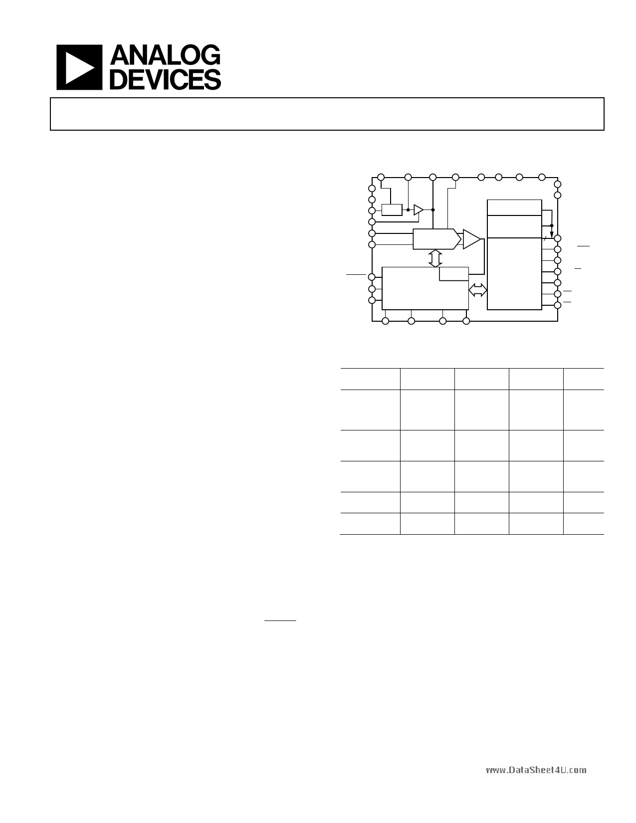
FUNCTIONAL BLOCK DIAGRAM
TEMP REFBUFIN REF REFGND VCC VEE DVDD DGND
AGND
AVDD
PDREF
PDBUF
IN+
IN–
REF
REF
AMP
SWITCHED
CAP DAC
CNVST
PD
RESET
CLOCK
CONTROL LOGIC AND
CALIBRATION CIRCUITRY
AD7951
SERIAL DATA
PORT
SERIAL
CONFIGURATION
PORT
14
PARALLEL
INTERFACE
OVDD
OGND
D[13:0]
SER/PAR
BYTESWAP
OB/2C
BUSY
RD
CS
WARP IMPULSE BIPOLAR TEN
Figure 1.
Table 1. 48-Lead 14-/16-/18-Bit PulSAR Selection
Type
100 kSPS to 500 kSPS to 570 kSPS to
250 kSPS
570 kSPS
1000 kSPS
Pseudo
Differential
AD7651
AD7660
AD7661
AD7650
AD7652
AD7664
AD7666
AD7653
AD7667
True Bipolar
AD7610
AD7663
AD7665
AD7951
AD7612
AD7671
True
Differential
AD7675
AD7676
AD7677
18-Bit, True
Differential
Multichannel/
Simultaneous
AD7678
AD7679
AD7654
AD7655
AD7674
>1000
kSPS
AD7621
AD7622
AD7623
AD7641
AD7643
Rev. 0
Information furnished by Analog Devices is believed to be accurate and reliable. However, no
responsibility is assumed by Analog Devices for its use, nor for any infringements of patents or other
rights of third parties that may result from its use. Specifications subject to change without notice. No
license is granted by implication or otherwise under any patent or patent rights of Analog Devices.
Trademarksandregisteredtrademarksarethepropertyoftheirrespectiveowners.
One Technology Way, P.O. Box 9106, Norwood, MA 02062-9106, U.S.A.
Tel: 781.329.4700
www.analog.com
Fax: 781.461.3113
©2006 Analog Devices, Inc. All rights reserved.
1 page 
www.DataSheet4U.com
AD7951
TIMING SPECIFICATIONS
AVDD = DVDD = 5 V; OVDD = 2.7 V to 5.5 V; VCC = 15 V; VEE = −15 V; VREF = 5 V; all specifications TMIN to TMAX, unless otherwise noted.
Table 3.
Parameter
CONVERSION AND RESET (See Figure 33 and Figure 34)
Convert Pulse Width
Time Between Conversions
Warp Mode/Normal Mode/Impulse Mode1
CNVST Low to BUSY High Delay
BUSY High All Modes (Except Master Serial Read After Convert)
Warp Mode/Normal Mode/Impulse Mode
Aperture Delay
End of Conversion to BUSY Low Delay
Conversion Time
Warp Mode/Normal Mode/Impulse Mode
Acquisition Time
Warp Mode/Normal Mode/Impulse Mode
RESET Pulse Width
PARALLEL INTERFACE MODES (See Figure 35 and Figure 37)
CNVST Low to DATA Valid Delay
Warp Mode/Normal Mode/Impulse Mode
DATA Valid to BUSY Low Delay
Bus Access Request to DATA Valid
Bus Relinquish Time
MASTER SERIAL INTERFACE MODES2 (See Figure 39 and Figure 40)
CS Low to SYNC Valid Delay
CS Low to Internal SDCLK Valid Delay2
CS Low to SDOUT Delay
CNVST Low to SYNC Delay, Read During Convert
Warp Mode/Normal Mode/Impulse Mode
SYNC Asserted to SDCLK First Edge Delay
Internal SDCLK Period3
Internal SDCLK High3
Internal SDCLK Low3
SDOUT Valid Setup Time3
SDOUT Valid Hold Time3
SDCLK Last Edge to SYNC Delay3
CS High to SYNC High-Z
CS High to Internal SDCLK High-Z
CS High to SDOUT High-Z
BUSY High in Master Serial Read After Convert3
CNVST Low to SYNC Delay, Read After Convert
Warp Mode/Normal Mode/Impulse Mode
SYNC Deasserted to BUSY Low Delay
Symbol Min
Typ
Max Unit
t1 10
t2
1/1.25/1.49
t3
t4
t5
t6 10
t7
2
t8
200
t9 10
ns
μs
35 ns
850/1100/1350 ns
ns
ns
850/1100/1350 ns
ns
ns
t10
t11 20
t12
t13 2
850/1100/1350
40
15
ns
ns
ns
ns
t14
t15
t16
t17
t18 3
t19 30
t20 15
t21 10
t22 4
t23 5
t24 5
t25
t26
t27
t28
t29
t30
50/290/530
10
10
10
45
See Table 4
10
10
10
710/950/1190
25
ns
ns
ns
ns
ns
ns
ns
ns
ns
ns
ns
ns
ns
ns
ns
ns
Rev. 0 | Page 5 of 32
5 Page 
www.DataSheet4U.com
AD7951
Pin No. Mnemonic
45 TEMP
46 REFBUFIN
47 PDREF
48 PDBUF
Type1
AO
AI
DI
DI
Description
Temperature Sensor Analog Output. Enabled when the internal reference is turned on
(PDREF = PDBUF = low). See the Temperature Sensor section.
Reference Buffer Input. When using an external reference with the internal reference buffer
(PDBUF = low, PDREF = high), applying 2.5 V on this pin produces 5 V on the REF pin.
See the Voltage Reference Input section.
Internal Reference Power-Down Input.
When low, the internal reference is enabled.
When high, the internal reference is powered down, and an external reference must be used.
Internal Reference Buffer Power-Down Input.
When low, the buffer is enabled (must be low when using internal reference).
When high, the buffer is powered-down.
1 AI = analog input; AI/O = bidirectional analog; AO = analog output; DI = digital input; DI/O = bidirectional digital; DO = digital output; P = power.
2 In serial configuration mode (SER/PAR = high, HW/SW = low), this input is programmed with the serial configuration register and this pin is a don’t care. See the
Hardware Configuration section and Software Configuration section.
Rev. 0 | Page 11 of 32
11 Page | ||
| Páginas | Total 30 Páginas | |
| PDF Descargar | [ Datasheet AD7951.PDF ] | |
Hoja de datos destacado
| Número de pieza | Descripción | Fabricantes |
| AD795 | Low Power/ Low Noise Precision FET Op Amp | Analog Devices |
| AD7951 | 14-Bit Programmable Input ADC | Analog Devices |
| AD7952 | Programmable Input PulSAR ADC | Analog Devices |
| Número de pieza | Descripción | Fabricantes |
| SLA6805M | High Voltage 3 phase Motor Driver IC. |
Sanken |
| SDC1742 | 12- and 14-Bit Hybrid Synchro / Resolver-to-Digital Converters. |
Analog Devices |
|
DataSheet.es es una pagina web que funciona como un repositorio de manuales o hoja de datos de muchos de los productos más populares, |
| DataSheet.es | 2020 | Privacy Policy | Contacto | Buscar |