|
|
PDF MC33762 Data sheet ( Hoja de datos )
| Número de pieza | MC33762 | |
| Descripción | Dual Ultra Low-Noise Low Dropout Voltage Regulator | |
| Fabricantes | ON Semiconductor | |
| Logotipo | ||
Hay una vista previa y un enlace de descarga de MC33762 (archivo pdf) en la parte inferior de esta página. Total 16 Páginas | ||
|
No Preview Available !
www.DataSheet4U.com
MC33762
Dual Ultra Low−Noise Low
Dropout Voltage Regulator
with 1.0 V ON/OFF Control
The MC33762 is a dual Low DropOut (LDO) regulator featuring
excellent noise performances. Thanks to its innovative design, the
circuit reaches an impressive 40 µVRMS noise level without an
external bypass capacitor. Housed in a small µ8 package, it represents
the ideal designer’s choice when space and noise are at premium.
The absence of external bandgap capacitor accelerates the response
time to a wake−up signal and keeps it within 40 µs, making the
MC33762 as a natural candidate for portable applications.
The MC33762 also hosts a novel architecture which prevents
excessive undershoots in the presence of fast transient bursts, as in any
bursting systems.
Finally, with a static line regulation better than −75 dB, it naturally
shields the downstream electronics from choppy lines.
Features
• Nominal Output Current of 80 mA with a 100 mA Peak Capability
• Ultra−Low Noise: 150 nV/√Hz @ 100 Hz, 40 µVRMS
100 Hz−100 kHz Typical, Iout = 60 mA, Co = 1.0 µF
• Fast Response Time from OFF to ON: 40 µs Typical
• Ready for 1.0 V Platforms: ON with a 900 mV High Level
• Typical Dropout of 90 mV @ 30 mA, 160 mV @ 80 mA
• Ripple Rejection: 70 dB @ 1.0 kHz
• 1.5% Output Precision @ 25°C
• Thermal Shutdown
• Vout Available at 2.5 V, 2.8 V, and 3.0 V
• Separate Dice for Each Regulator Provides Maximum Isolation
Between Regulators
• Operating Range from −40 to +85°C
Applications
• Noise Sensitive Circuits: VCOs RF Stages, etc.
• Bursting Systems (TDMA Phones)
• All Battery Operated Devices
http://onsemi.com
8
1
Micro8t
DM SUFFIX
CASE 846A
PIN CONFIGURATION AND
MARKING DIAGRAM
Gnd1 1
En1 2
Gnd2 3
En2 4
8 Vout1
7 VCC1
6 Vout2
5 VCC2
(Top View)
xxxx = Version
Y = Year
WW = Work Week
ORDERING INFORMATION
See detailed ordering and shipping information in the package
dimensions section on page 14 of this data sheet.
© Semiconductor Components Industries, LLC, 2003
July, 2003 − Rev. 4
1
Publication Order Number:
MC33762/D
1 page 
MC33762
DEFINITIONS
Load Regulation
The change in output voltage for a change in output
current at a constant chip temperature.
Dropout Voltage
The input/output differential at which the regulator output
no longer maintains regulation against further reductions in
input voltage. Measured when the output drops 100 mV
below its nominal value (which is measured at 1.0 V
differential value). The dropout level is affected by the chip
temperature, load current and minimum input supply
requirements.
Output Noise Voltage
This is the integrated value of the output noise over a
specified frequency range. Input voltage and output current
are kept constant during the measurement. Results are
expressed in µVRMS.
Maximum Power Dissipation
The maximum total dissipation for which the regulator
will operate within its specs.
Quiescent Current
The quiescent current is the current which flows through
the ground when the LDO operates without a load on its
output: internal IC operation, bias etc. When the LDO
becomes loaded, this term is called the Ground current. It is
actually the difference between the input current (measured
through the LDO input pin) and the output current.
Line Regulation
The change in output voltage for a change in input voltage.
The measurement is made under conditions of low
dissipation or by using pulse technique such that the average
chip temperature is not significantly affected. One usually
distinguishes static line regulation or DC line regulation (a
DC step in the input voltage generates a corresponding step
in the output voltage) from ripple rejection or audio
susceptibility where the input is combined with a frequency
generator to sweep from a few hertz up to a defined
boundary while the output amplitude is monitored.
Thermal Protection
Internal thermal shutdown circuitry is provided to protect
the integrated circuit in the event that the maximum junction
temperature is exceeded. When activated at typically 125°C,
the regulator turns off. This feature is provided to prevent
catastrophic failures from accidental overheating.
Maximum Package Power Dissipation
The maximum power package power dissipation is the
power dissipation level at which the junction temperature
reaches its maximum operating value, i.e. 125°C.
Depending on the ambient temperature, it is possible to
calculate the maximum power dissipation and thus the
maximum available output current.
http://onsemi.com
5
5 Page 
MC33762
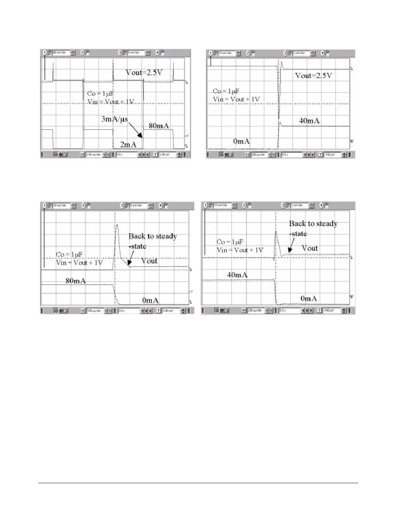
TYPICAL TRANSIENT RESPONSES
Figure 13. Output is Pulsed from 2.0 mA to 80 mA
Figure 14. Discharge Effects from 0 to 40 mA
Figure 15. Load Transient Improvement Effect
Figure 16. Load Transient Improvement Effect
http://onsemi.com
11
11 Page | ||
| Páginas | Total 16 Páginas | |
| PDF Descargar | [ Datasheet MC33762.PDF ] | |
Hoja de datos destacado
| Número de pieza | Descripción | Fabricantes |
| MC33761 | Ultra Low-Noise Low Dropout Voltage Regulator with 1V ON/OFF Control | ON Semiconductor |
| MC33762 | Dual Ultra Low-Noise Low Dropout Voltage Regulator | ON Semiconductor |
| MC33765 | Very Low Dropout/Ultra Low Noise 5 Outputs Voltage Regulator | ON Semiconductor |
| Número de pieza | Descripción | Fabricantes |
| SLA6805M | High Voltage 3 phase Motor Driver IC. |
Sanken |
| SDC1742 | 12- and 14-Bit Hybrid Synchro / Resolver-to-Digital Converters. |
Analog Devices |
|
DataSheet.es es una pagina web que funciona como un repositorio de manuales o hoja de datos de muchos de los productos más populares, |
| DataSheet.es | 2020 | Privacy Policy | Contacto | Buscar |
