|
|
|
PDF BP5718A12 Data sheet ( Hoja de datos )
| Número de pieza | BP5718A12 | |
| Descripción | AC-DC Converter | |
| Fabricantes | ROHM Semiconductor | |
| Logotipo | ||
Hay una vista previa y un enlace de descarga de BP5718A12 (archivo pdf) en la parte inferior de esta página. Total 3 Páginas | ||
|
No Preview Available !
www.DataSheet4U.com
Insulation Type AC-DC Converter
AC 100V input, 12 V/1000 mA output
BP5718A12
Absolute Maximum Ratings
Parameter
Symbol
Limits
Unit
Conditions
Pin 11 input voltage
VD
500
V
Pin 7,9 input voltage
VDD
25
V
Pin 11 input Current
ID
500 mA
Pin 8 input Current
IDD
10
mA
Output power
Po 13 W
Withstand voltage
VI
2.5
KV 1 sec (between primary and secondary)
Maximum allowable
surface temperature
Tcmax
105
°C Ambient temperature + module
self-heating Tcmax
Operating
temperature range
Topr −25 to +80
°C
Storage temperature
range
Tstg −40 to +105
°C
Electrical Characteristics
Parameter
Symbol Min. Typ. Max.
Pin 11 input voltage VD
−
− 350
Operating power
voltage(Pin 7)
VDD
8.8
12
20
Rated output voltage Vo
11.4 12.0 12.6
Rated output current Io 0 − 1000
Line regulation
∆Vr −
5 200
Load regulation
∆VI −
58 200
Output ripple voltage ∆γ
− 135 500
Power conversion
efficiency
η 75 83
−
*1: The operation starting voltage is between 15.5 and 17.5 V.
*2: Pulsating noise is not included.
Unit
V
V
V
mA
mV
mV
mVpp
%
Conditions
Note 2:Io=1000mA
DC, Io=1000mA *1
See derating curve
Vi=113V to 195VDC
Io=1000mA
Io=50mA to 1000mA
*2
Sample Application Circuit
Vi(+) R5
AC100V
ZNR
F1
D7
C4 C7 R2
Vi(-)
Use a fuse for safety
87
T1 D1
39
R1 C2
C1
D2 1 1
D3 D5
C3 4
5
6
7
C6
C5
11
Vo1:12V/850mA
GND1
Vo2:18V/100mA
GND2
21
BP5718A12
Pin Terminal
No. name
Terminal function
Secondary 12V output
voltage control terminal.
1 Vo Insert a 1000µF output
smoothing capacitor before the
GND for use.
2
GND
Secondary 12V output GND
terminal.
6
Vin(-)
Primary input negative
terminal.
7 VDD Internal circuit power terminal.
Start-up terminal. Connect to
8 Vs Vi (+) through an external
resistor (1.5MΩ).
9 NC NC pin.
11
VD
Drain terminal for the buiit-in
FET.
6 Verify proper operation under actual conditions
before use. In particular, confirm that
the load current does not exceed the maximum
rating.
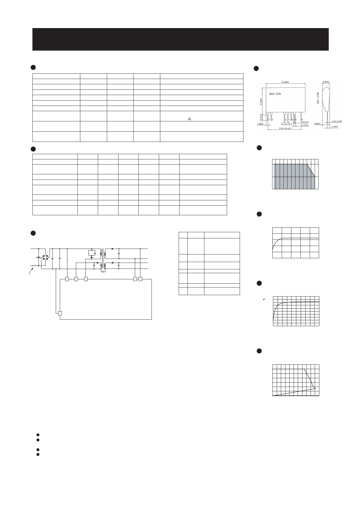
Dimensions (mm)
Derating Curve
12
6 Operation Range
-30-20-10 0 10 20 30 40 50 60 70 80 90
Ambient Temperature Ta(°C)
Switching Frequency
100
80
60
40
20
0
0
200 400 600 800 1000
Output Current Io(mA)
Conversion Efficiency
100
90
80
70
60
50
40
30
20
10
0
0
500 1000
Output Current Io(mA)
External Component Settings
C1: Output Capacitor
C2: Noise Reduction Capacitor
C3: VDD Capacitor
C4: Input Capacitor
C5: Noise Reduction Capacitor
C6: Output Capacitor
C7: Noise Reduction Capacitor
1000µF/35V low-impedance
capacitor for power supply
2200pF/400V
10µF/50V low-impedance
capacitor for power supply
100µF/250V
(optional)
100µF/35V low-impedance
(optional)
D3: Rectifier Diode
80V/0.1A
D5: Rectifier Diode
100V/1A
D7: Diode Bridge
800V/1A
R1: Resistor 1
100kΩ±5%, 3W, 300VDC or
higher ruted voltage
R2: Resistor 2
1.5MΩ±5%, 0.25W, 300VDC or
higher ruted voltage.
R5: Noise Reduction Resistor (optional)
T1: Switching Transformer
Load Regulation
14.0
12.0
10.0
8.0
6.0
4.0
2.0
0.0
0
1000
Output Current Io(mA)
2200
D1: Rectifier Diode
60V/6A
F1: Fuse
Use a fuse for safety
D2: Rectifier Diode
1kV/1A
ZNR: Varistor
A varistor is required in order to
protect against lightning surges and
Operation Notes
static electricity.
An excessively large capacitance at C1 may cause the output to become inactive. Therefore, a capacitance between 1000 and 2200µF is recommended, with a rise time of 10ms or less.
The capacitance of C3 should be 10µF, since an excessively small value will result in malfunction. The activation time is defined as: t(sec)=R2×C3×ln[1-17/(VI-30µA×R2)], where VI is the
DC voltage after smoothing.
The resistance of R2 should be 1.5MΩ, since an excessively small value will result in malfunction.
Overcurrent (reset type) and overvoltage (latch type) protection circuits are built in, preventing damage from occurring due to unexpected conditions. The overvoltage protection circuit shuts
down operation once VDD exceeds 20V. In order to reset the input capacitor C4 must be discharged and the power turned back on.
1 page | ||
| Páginas | Total 3 Páginas | |
| PDF Descargar | [ Datasheet BP5718A12.PDF ] | |
Hoja de datos destacado
| Número de pieza | Descripción | Fabricantes |
| BP5718A12 | AC-DC Converter | ROHM Semiconductor |
| Número de pieza | Descripción | Fabricantes |
| SLA6805M | High Voltage 3 phase Motor Driver IC. |
Sanken |
| SDC1742 | 12- and 14-Bit Hybrid Synchro / Resolver-to-Digital Converters. |
Analog Devices |
|
DataSheet.es es una pagina web que funciona como un repositorio de manuales o hoja de datos de muchos de los productos más populares, |
| DataSheet.es | 2020 | Privacy Policy | Contacto | Buscar |