|
|
PDF TZA3036 Data sheet ( Hoja de datos )
| Número de pieza | TZA3036 | |
| Descripción | SDH/SONET STM1/OC3 transimpedance amplifier | |
| Fabricantes | NXP Semiconductors | |
| Logotipo | ||
Hay una vista previa y un enlace de descarga de TZA3036 (archivo pdf) en la parte inferior de esta página. Total 15 Páginas | ||
|
No Preview Available !
www.DataSheet4U.com
TZA3036
SDH/SONET STM1/OC3 transimpedance amplifier
Rev. 01 — 24 March 2006
Product data sheet
1. General description
The TZA3036 is a transimpedance amplifier with Automatic Gain Control (AGC), designed
to be used in STM1/OC3 fiber optic links. It amplifies the current generated by a photo
detector (PIN diode or avalanche photodiode) and converts it to a differential output
voltage. It offers a current mirror of average photo current for RSSI monitoring to be used
in SFF-8472 compliant modules.
The low noise characteristics makes it suitable for STM1/OC3 applications, but also for
FTTx applications.
CAUTION
This device is sensitive to ElectroStatic Discharge (ESD). Therefore care should be taken
during transport and handling.
2. Features
I Low equivalent input noise, typically 12 nA (RMS)
I Wide dynamic range, typically 0.18 µA to 1.5 mA (p-p)
I Differential transimpedance of 69 kΩ (typical)
I Bandwidth from DC to 160 MHz (typical)
I Differential outputs
I On-chip (AGC) with possibility of external control
I Single supply voltage 3.3 V; range 2.9 V to 3.6 V
I Bias voltage for PIN diode
I On-chip current mirror of average photo current for RSSI monitoring
I Identical ports available on both sides of die for easy bond layout and RF polarity
selection
3. Applications
I Digital fiber optic receiver modules in telecommunications transmission systems, in
high speed data networks or in FTTx systems.
1 page 
www.DataSheet4U.com
Philips Semiconductors
TZA3036
SDH/SONET STM1/OC3 transimpedance amplifier
The parasitic capacitance can be minimized through:
1. Reducing the capacitance of the PIN diode. This is achieved by proper choice of PIN
diode and typically a high reverse voltage.
2. Reducing the parasitics around the input pad. This is achieved by placing the PIN
diode as close as possible to the TIA.
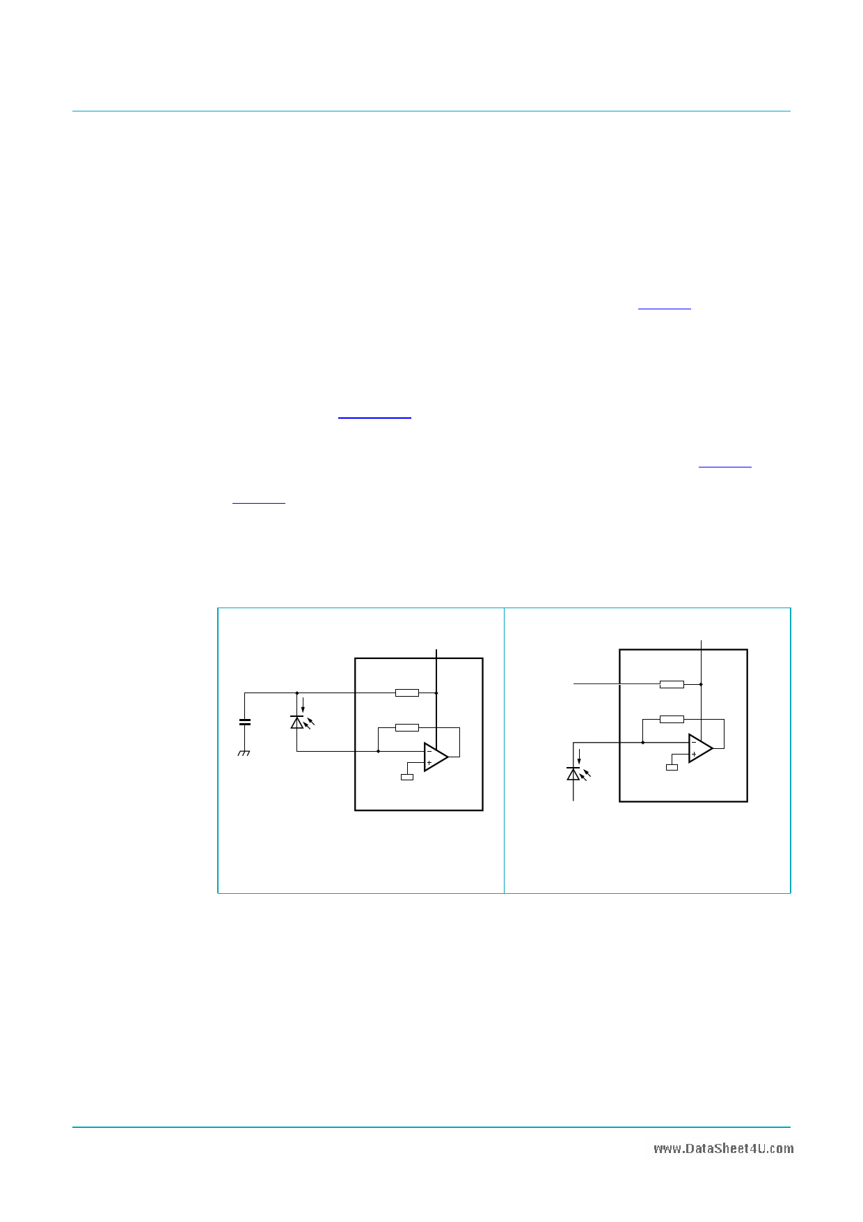
The PIN diode can be biased with a positive or a negative voltage. Figure 3 shows the PIN
diode biased positively, using the on-chip bias pad DREF. The voltage at DREF is derived
from VCC by a low-pass filter comprising internal resistor RDREF and external capacitor C2
which decouples any supply voltage noise. The value of external capacitor C2 affects the
value of PSRR and should have a minimum value of 470 pF. Increasing this value
improves the value of PSRR. The current through RDREF is measured and sourced at pad
IDREF_MON, see Section 7.3.
If the biasing for the PIN diode is done external to the IC, pad DREF can be left
unconnected. If a negative bias voltage is used, the configuration shown in Figure 4 can
be used. In this configuration, the direction of the signal current is reversed to that shown
in Figure 3. It is essential that in these applications, the PIN diode bias voltage is filtered to
achieve the best sensitivity.
For maximum freedom on bonding location, 2 outputs are available for DREF (pads 1
and 3). These are internally connected. Both outputs can be used if necessary. If only one
is used, the other can be left open.
C2
470 pF
VCC
DREF 1 or 3 RDREF
IPIN
290 Ω
4 or 17
IPHOTO 2
TZA3036
001aad077
Fig 3. The PIN diode connected between
the input and pad DREF
VCC
DREF 1 or 3 RDREF
290 Ω
4 or 17
IPHOTO 2
IPIN
negative
bias voltage
TZA3036
001aad078
Fig 4. The PIN diode connected between
the input and a negative supply
voltage
TZA3036_1
Product data sheet
Rev. 01 — 24 March 2006
© Koninklijke Philips Electronics N.V. 2006. All rights reserved.
5 of 15
5 Page 
xxxx xxxxxxxxxxxxxxxxxxxxxxxxxxxxxx x xxxxxxxxxxxxxx xxxxxxxxxx xxx xxxxxx xxxxxxxxxxxxxxxxxxxxxxx xxxxxxxxxxxxxxxxxxxxxx
xxxxx xxxxxx xx xxxxxxxxxxxxxxxxxxxxxxxxxxxxx xxxxxxxxxxxxxxxxxxxxxx xxxxxxxxxxx xxxxxxx xxxxxxxxxxxxxxxxxxx
xxxxxxxxxxxxxxxx xxxxxxxxxxxxxx xxxxxx xx xxxxxxxxxxxxxxxxxxxxxxxxxxxxxxxx xxxxxxxxxxxxxxxxxxxxxxxx xxxxxxx
xxxxxxxxxxxxxxxxxxxxxxxxxxxxxxxxxxxxxxxxxxxxxx xxxxxxxxxxx xxxxx x x
NETWORK ANALYZER
DC-IN
PATTERN
GENERATOR DATA
CLOCK
S-PARAMETER TEST SET
PORT1
PORT2
Zo = 50 Ω
Zo= 50 Ω
VCC
22 nF
55 Ω
4 or 17
8 or 14 OUT
22 nF
8.2
kΩ
2200 Ω
R
TZA3036
IPHOTO
2
OUTQ 22 nF
7 or 13
9, 10, 11, 12
GND
SAMPLING OSCILLOSCOPE
12
Zo = 50 Ω
TRIGGER
INPUT
001aad083
Total impedance of the test circuit (Ztot(tc)) is calculated by the equation Ztot(tc) = s21 × (R + Zi) × 2, where s21 is the insertion loss of ports 1 and 2.
Typical values: R = 2200 Ω, Zi = 300 Ω.
Fig 9. Test circuit
11 Page | ||
| Páginas | Total 15 Páginas | |
| PDF Descargar | [ Datasheet TZA3036.PDF ] | |
Hoja de datos destacado
| Número de pieza | Descripción | Fabricantes |
| TZA3030 | SDH/SONET STM1/OC3 optical receiver | NXP Semiconductors |
| TZA3031 | SDH/SONET STM1/OC3 and STM4/OC12 transceiver | NXP Semiconductors |
| TZA3031AHL | SDH/SONET STM1/OC3 laser drivers | NXP Semiconductors |
| TZA3031BHL | SDH/SONET STM1/OC3 laser drivers | NXP Semiconductors |
| Número de pieza | Descripción | Fabricantes |
| SLA6805M | High Voltage 3 phase Motor Driver IC. |
Sanken |
| SDC1742 | 12- and 14-Bit Hybrid Synchro / Resolver-to-Digital Converters. |
Analog Devices |
|
DataSheet.es es una pagina web que funciona como un repositorio de manuales o hoja de datos de muchos de los productos más populares, |
| DataSheet.es | 2020 | Privacy Policy | Contacto | Buscar |
