|
|
|
PDF ADCMP605 Data sheet ( Hoja de datos )
| Número de pieza | ADCMP605 | |
| Descripción | (ADCMP604 / ADCMP605) Single-Supply LVDS Comparators | |
| Fabricantes | Analog Devices | |
| Logotipo | ||
Hay una vista previa y un enlace de descarga de ADCMP605 (archivo pdf) en la parte inferior de esta página. Total 16 Páginas | ||
|
No Preview Available !
www.DataSheet4U.com
Rail-to-Rail, Very Fast, 2.5 V to 5.5 V,
Single-Supply LVDS Comparators
ADCMP604/ADCMP605
FEATURES
Fully specified rail to rail at VCC = 2.5 V to 5.5 V
Input common-mode voltage from −0.2 V to VCC + 0.2 V
Low glitch LVDS-compatible output stage
1.6 ns propagation delay
37 mW at 2.5 V
Shutdown pin
Single-pin control for programmable hysteresis and latch
Power supply rejection > 60 dB
−40°C to +125°C operation
APPLICATIONS
High speed instrumentation
Clock and data signal restoration
Logic level shifting or translation
Pulse spectroscopy
High speed line receivers
Threshold detection
Peak and zero-crossing detectors
High speed trigger circuitry
Pulse-width modulators
Current-/voltage-controlled oscillators
Automatic test equipment (ATE)
GENERAL DESCRIPTION
The ADCMP604 and ADCMP605 are very fast comparators
fabricated on Analog Devices, Inc.’s, proprietary XFCB2
process. This family of comparators is exceptionally versatile
and easy to use. Features include an input range from VEE − 0.5
V to VCC + 0.2 V, low noise, LVDS-compatible output drivers,
and TTL/CMOS latch inputs with adjustable hysteresis and/or
shutdown inputs.
The devices offer 1.5 ns propagation delays with 1 ps rms
random jitter (RJ). Overdrive and slew rate dispersion are
typically less than 50 ps.
A flexible power supply scheme allows the devices to operate
with a single +2.5 V positive supply and a −0.5 V to +3.0 V
input signal range up to a +5.5 V positive supply with a −0.5 V
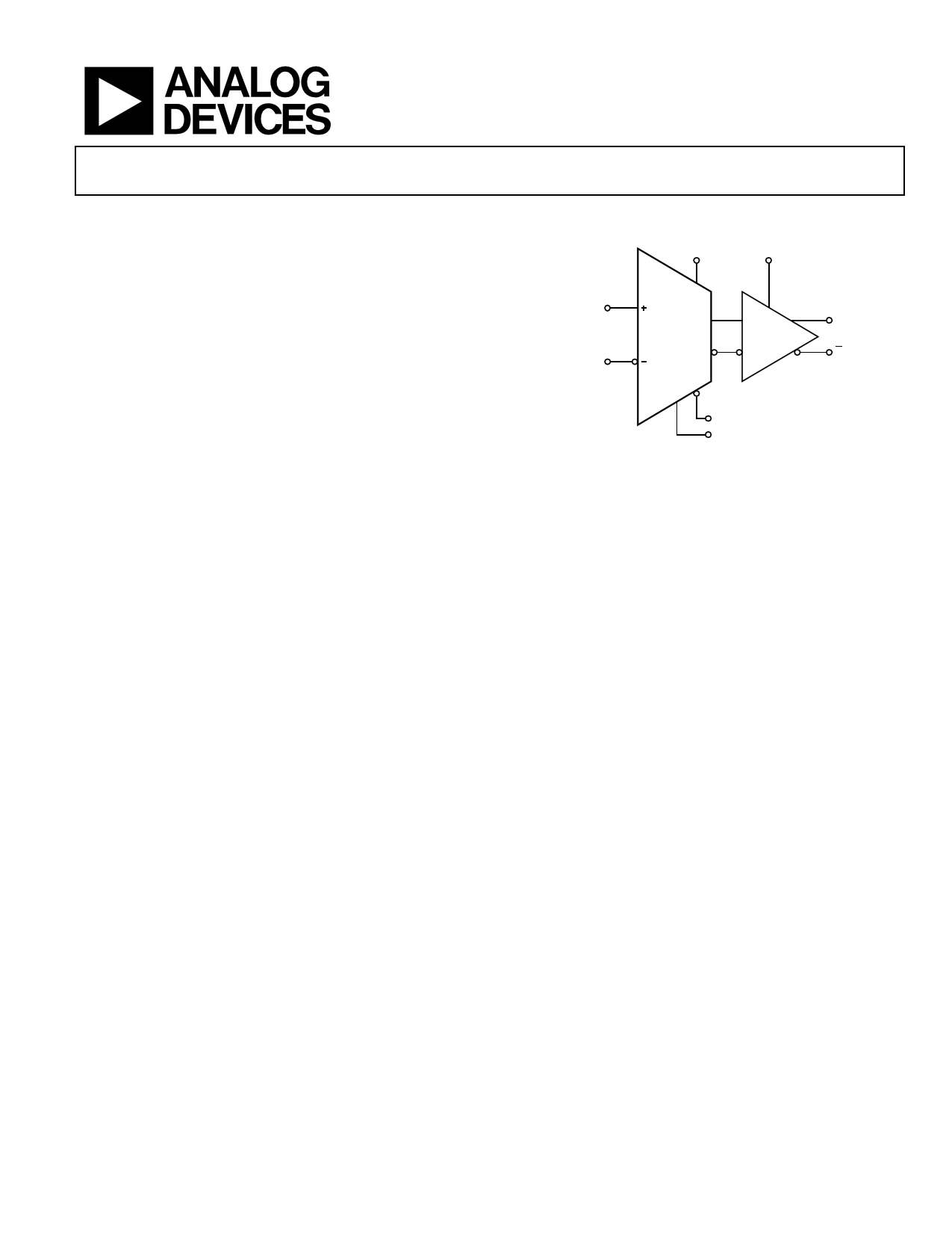
FUNCTIONAL BLOCK DIAGRAM
VCCI
VCCO
(ADCMP605 ONLY)
VP
NONINVERTING
INPUT
VN
INVERTING
INPUT
ADCMP604/
ADCMP605
LVDS
Q OUTPUT
Q OUTPUT
LE/HYS INPUT (ADCMP605
SDN INPUT
ONLY)
Figure 1.
to +6 V input signal range. Split input/output supplies, with no
sequencing restrictions on the ADCMP605, support a wide
input signal range with greatly reduced power consumption.
The LVDS-compatible output stage is designed to drive any
standard LVDS input. The comparator input stage offers robust
protection against large input overdrive, and the outputs do not
phase reverse when the valid input signal range is exceeded.
High speed latch and programmable hysteresis features are also
provided in a unique single-pin control option.
The ADCMP604 is available in a 6-lead SC70 package. The
ADCMP605 is available in a 12-lead LFCSP.
Rev. 0
Information furnished by Analog Devices is believed to be accurate and reliable. However, no
responsibility is assumed by Analog Devices for its use, nor for any infringements of patents or other
rights of third parties that may result from its use. Specifications subject to change without notice. No
license is granted by implication or otherwise under any patent or patent rights of Analog Devices.
Trademarksandregisteredtrademarksarethepropertyoftheirrespectiveowners.
One Technology Way, P.O. Box 9106, Norwood, MA 02062-9106, U.S.A.
Tel: 781.329.4700
www.analog.com
Fax: 781.461.3113
©2006 Analog Devices, Inc. All rights reserved.
1 page 
ADCMP604/ADCMP605
TIMING INFORMATION
Figure 2 illustrates the ADCMP604/ADCMP605 latch timing relationships. Table 2 provides definitions of the terms shown in Figure 2.
LATCH ENABLE
tS
tH
tPL
DIFFERENTIAL
INPUT VOLTAGE
VIN
VOD
Q OUTPUT
Q OUTPUT
tPDL
tPLOH
tPDH
tF
tR
Figure 2. System Timing Diagram
tPLOL
1.1V
VN ± VOS
50%
50%
Table 2. Timing Descriptions
Symbol Timing
tPDH Input to output high
delay
tPDL Input to output low
delay
tPLOH Latch enable to output
high delay
tPLOL Latch enable to output
low delay
tH Minimum hold time
tPL Minimum latch enable
pulse width
tS Minimum setup time
tR Output rise time
tF Output fall time
VOD Voltage overdrive
Description
Propagation delay measured from the time the input signal crosses the reference (± the input offset
voltage) to the 50% point of an output low-to-high transition.
Propagation delay measured from the time the input signal crosses the reference (± the input offset
voltage) to the 50% point of an output high-to-low transition.
Propagation delay measured from the 50% point of the latch enable signal low-to-high transition to
the 50% point of an output low-to-high transition.
Propagation delay measured from the 50% point of the latch enable signal low-to-high transition to
the 50% point of an output high-to-low transition.
Minimum time after the negative transition of the latch enable signal that the input signal must
remain unchanged to be acquired and held at the outputs.
Minimum time that the latch enable signal must be high to acquire an input signal change.
Minimum time before the negative transition of the latch enable signal occurs that an input signal
change must be present to be acquired and held at the outputs.
Amount of time required to transition from a low to a high output as measured at the 20% and 80%
points.
Amount of time required to transition from a high to a low output as measured at the 20% and 80%
points.
Difference between the input voltages VA and VB.
Rev. 0 | Page 5 of 16
5 Page 
The ADCMP604 and ADCMP605 dispersion is typically < 1.6 ns
as the overdrive varies from 10 mV to 125 mV. This specification
applies to both positive and negative signals because each the
ADCMP604 and ADCMP605 have substantially equal delays for
positive-going and negative-going inputs and very low output
skews.
500mV OVERDRIVE
INPUT VOLTAGE
10mV OVERDRIVE
VN ± VOS
DISPERSION
Q/Q OUTPUT
Figure 17. Propagation Delay—Overdrive Dispersion
INPUT VOLTAGE
1V/ns
10V/ns
VN ± VOS
DISPERSION
Q/Q OUTPUT
Figure 18. Propagation Delay—Slew Rate Dispersion
COMPARATOR HYSTERESIS
The addition of hysteresis to a comparator is often desirable in a
noisy environment, or when the differential input amplitudes
are relatively small or slow moving. The transfer function for a
comparator with Hysteresis is shown in Figure 19. As the input
voltage approaches the threshold (0.0 V, in this example) from
below the threshold region in a positive direction, the
comparator switches from low to high when the input crosses
+VH/2. The new switching threshold becomes −VH/2. The
comparator remains in the high state until the threshold, −VH/2,
is crossed from below the threshold region in a negative direction.
In this manner, noise or feedback output signals centered on
0.0 V input cannot cause the comparator to switch states unless it
exceeds the region bounded by ±VH/2.
ADCMP604/ADCMP605
OUTPUT
VOH
VOL
–VH 0
2
INPUT
+VH
2
Figure 19. Comparator Hysteresis Transfer Function
The customary technique for introducing hysteresis into a
comparator uses positive feedback from the output back to the
input. One limitation of this approach is that the amount of
hysteresis varies with the output logic levels, resulting in
hysteresis that is not symmetric about the threshold. The
external feedback network can also introduce significant
parasitics that reduce high speed performance and induce
oscillation in some cases.
The ADCMP605 comparator offers a programmable hysteresis
feature that significantly improves accuracy and stability.
Connecting an external pull-down resistor or a current source
from the LE/HYS pin to GND, varies the amount of hysteresis
in a predictable and stable manner. Leaving the LE/HYS pin
disconnected or driving it high removes hysteresis. The
maximum hysteresis that can be applied using this pin is
approximately 160 mV. Figure 20 illustrates the amount of
hysteresis applied as a function of external resistor value.
Figure 11 illustrates hysteresis as a function of current.
The hysteresis control pin appears as a 1.25 V bias voltage seen
through a series resistance of 7 kΩ ± 20% throughout the
hysteresis control range. The advantages of applying hysteresis
in this manner are improved accuracy, improved stability,
reduced component count, and maximum versatility. An
external bypass capacitor is not recommended on the HYS pin
because it would likely degrade the jitter performance of the
device and impair the latch function. As described in the
Using/Disabling the Latch Feature section, hysteresis control
need not compromise the latch function.
Rev. 0 | Page 11 of 16
11 Page | ||
| Páginas | Total 16 Páginas | |
| PDF Descargar | [ Datasheet ADCMP605.PDF ] | |
Hoja de datos destacado
| Número de pieza | Descripción | Fabricantes |
| ADCMP600 | (ADCMP600 - ADCMP602) Single-Supply TTL/CMOS Comparator | Analog Devices |
| ADCMP601 | (ADCMP600 - ADCMP602) Single-Supply TTL/CMOS Comparator | Analog Devices |
| ADCMP602 | (ADCMP600 - ADCMP602) Single-Supply TTL/CMOS Comparator | Analog Devices |
| ADCMP603 | Single-Supply TTL/CMOS Comparator | Analog Devices |
| Número de pieza | Descripción | Fabricantes |
| SLA6805M | High Voltage 3 phase Motor Driver IC. |
Sanken |
| SDC1742 | 12- and 14-Bit Hybrid Synchro / Resolver-to-Digital Converters. |
Analog Devices |
|
DataSheet.es es una pagina web que funciona como un repositorio de manuales o hoja de datos de muchos de los productos más populares, |
| DataSheet.es | 2020 | Privacy Policy | Contacto | Buscar |