|
|
|
PDF ADP3120A Data sheet ( Hoja de datos )
| Número de pieza | ADP3120A | |
| Descripción | MOSFET Driver | |
| Fabricantes | Analog Devices | |
| Logotipo | ||
Hay una vista previa y un enlace de descarga de ADP3120A (archivo pdf) en la parte inferior de esta página. Total 16 Páginas | ||
|
No Preview Available !
www.DataSheet4U.com
FEATURES
All-in-one synchronous buck driver
Bootstrapped high-side drive
One PWM signal generates both drives
Anticross conduction protection circuitry
OD for disabling the driver outputs
Meets CPU VR requirement when used with
Analog Devices Flex -Mode™1 controller
APPLICATIONS
Multiphase desktop CPU supplies
Single-supply synchronous buck converters
Dual Bootstrapped, 12 V MOSFET
Driver with Output Disable
ADP3120A
GENERAL DESCRIPTION
The ADP3120A is a dual, high voltage MOSFET driver
optimized for driving two N-channel MOSFETs, the two switches
in a nonisolated synchronous buck power converter. Each
driver is capable of driving a 3000 pF load with a 45 ns propaga-
tion delay and a 25 ns transition time. One of the drivers can be
bootstrapped and is designed to handle the high voltage slew
rate associated with floating high-side gate drivers. The
ADP3120A includes overlapping drive protection to prevent
shoot-through current in the external MOSFETs.
The OD pin shuts off both the high-side and the low-side
MOSFETs to prevent rapid output capacitor discharge during
system shutdown.
The ADP3120A is specified over the commercial temperature
range of 0°C to 85°C and is available in 8-lead SOIC_N and
8-lead LFCSP_VD packages.
1 Flex-Mode is protected by U.S. Patent 6683441; other patents pending.
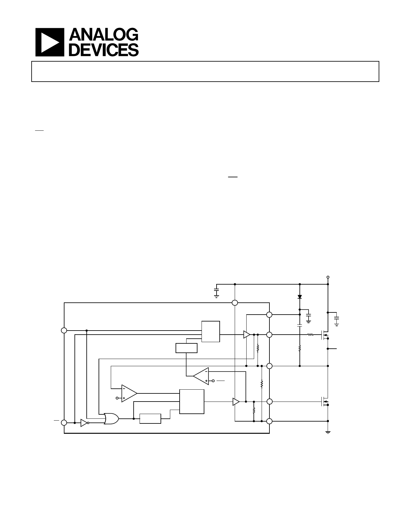
FUNCTIONAL BLOCK DIAGRAM
12V
ADP3120A
IN 2
VCC
4
DELAY
LATCH
R1
R2 Q
S
OD 3
CMP
1V
DELAY
CMP
VCC
6
CONTROL
LOGIC
Figure 1.
D1
BST
1
CBST1
DRVH
8
CBST2
RG
Q1
SW
7
RBST
TO
INDUCTOR
DRVL
5
PGND
6
Q2
Rev. 0
Information furnished by Analog Devices is believed to be accurate and reliable. However, no
responsibility is assumed by Analog Devices for its use, nor for any infringements of patents or other
rights of third parties that may result from its use. Specifications subject to change without notice. No
license is granted by implication or otherwise under any patent or patent rights of Analog Devices.
Trademarksandregisteredtrademarksarethepropertyoftheirrespectiveowners.
One Technology Way, P.O. Box 9106, Norwood, MA 02062-9106, U.S.A.
Tel: 781.329.4700
www.analog.com
Fax: 781.461.3113
©2006 Analog Devices, Inc. All rights reserved.
1 page 
PIN CONFIGURATIONS AND FUNCTION DESCRIPTIONS
ADP3120A
BST 1
IN 2
OD 3
VCC 4
ADP3120A
TOP VIEW
(Not to Scale)
8 DRVH
7 SW
6 PGND
5 DRVL
Figure 2. 8-Lead SOIC_N Pin Configuration
BST 1
IN 2
OD 3
VCC 4
PIN 1
INDICATOR
ADP3120A
TOP VIEW
(Not to Scale)
8 DRVH
7 SW
6 PGND
5 DRVL
Figure 3. 8-Lead LFCSP_VD Pin Configuration
Table 3. Pin Function Descriptions
Pin No. Mnemonic Description
1 BST
Upper MOSFET Floating Bootstrap Supply. A capacitor connected between the BST and SW pins holds this
bootstrapped voltage for the high-side MOSFET while it is switching.
2 IN
Logic Level PWM Input. This pin has primary control of the drive outputs. In normal operation, pulling this pin
low turns on the low-side driver; pulling it high turns on the high-side driver.
3 OD
Output Disable. When low, this pin disables normal operation, forcing DRVH and DRVL low.
4 VCC
Input Supply. This pin should be bypassed to PGND with an ~1 μF ceramic capacitor.
5 DRVL
Synchronous Rectifier Drive. Output drive for the lower (synchronous rectifier) MOSFET.
6 PGND
Power Ground. This pin should be closely connected to the source of the lower MOSFET.
7 SW
Switch Node Connection. This pin is connected to the buck switching node, close to the upper MOSFET source.
It is the floating return for the upper MOSFET drive signal. It is also used to monitor the switched voltage to
prevent the lower MOSFET from turning on until the voltage is below ~1 V.
8 DRVH
Buck Drive. Output drive for the upper (buck) MOSFET.
Rev. 0 | Page 5 of 16
5 Page 
ADP3120A
The MOSFET vendor should provide a rating for the maximum
voltage slew rate at drain current around which this can be
designed. Once this specification is obtained, determine the
maximum current expected in the MOSFET by
( )I MAX = IDC ( per phase) + VCC −VOUT
× DMAX
f MAX × LOUT
(5)
where:
DMAX is determined for the VR controller being used with
the driver. This current is divided roughly equally between
MOSFETs if more than one is used (assume a worst-case
mismatch of 30% for design margin).
LOUT is the output inductor value.
When producing the design, there is no exact method for
calculating the dV/dt due to the parasitic effects in the external
MOSFETs as well as the PCB. However, it can be measured to
determine if it is safe. If it appears that the dV/dt is too fast, an
optional gate resistor can be added between DRVH and the
high-side MOSFETs. This resistor slows down the dV/dt, but it
increases the switching losses in the high-side MOSFETs. The
ADP3120A is optimally designed with an internal drive
impedance that works with most MOSFETs to switch them
efficiently, yet minimizes dV/dt. However, some high speed
MOSFETs can require this external gate resistor depending on
the currents being switched in the MOSFET.
LOW-SIDE (SYNCHRONOUS) MOSFETS
The low-side MOSFETs are usually selected to have a low on
resistance to minimize conduction losses. This usually implies a
large input gate capacitance and gate charge. The first concern is
to make sure the power delivery from the ADP3120A DRVL
does not exceed the thermal rating of the driver (see the
ADP3186, ADP3188, or ADP3189 data sheets for Flex-Mode
controller details).
The next concern for the low-side MOSFETs is to prevent
them from being inadvertently switched on when the high-side
MOSFET turns on. This occurs due to the drain-gate (Miller
capacitance, also specified as Crss capacitance) of the MOSFET.
When the drain of the low-side MOSFET is switched to VCC by
the high-side turning on (at a dV/dt rate), the internal gate of
the low-side MOSFET is pulled up by an amount roughly equal
to VCC × (Crss/Ciss). It is important to make sure this does not put
the MOSFET into conduction.
Another consideration is the nonoverlap circuitry of the
ADP3120A that attempts to minimize the nonoverlap period.
During the state of the high-side turning off to low-side turning
on, the SW pin is monitored (as well as the conditions of SW
prior to switching) to adequately prevent overlap.
However, during the low-side turn-off to high-side turn-on,
the SW pin does not contain information for determining
the proper switching time, so the state of the DRVL pin is
monitored to go below one sixth of VCC; then, a delay is added.
Due to the Miller capacitance and internal delays of the low-
side MOSFET gate, ensure that the Miller-to-input capacitance
ratio is low enough, and that the low-side MOSFET internal
delays are not so large as to allow accidental turn-on of the low-
side when the high-side turns on.
Contact ADI for an updated list of recommended low-side
MOSFETs.
PC BOARD LAYOUT CONSIDERATIONS
Use these general guidelines when designing printed circuit
boards:
• Trace out the high current paths and use short, wide
(>20 mil) traces to make these connections.
• Minimize trace inductance between DRVH and DRVL
outputs and MOSFET gates.
• Connect the PGND pin of the ADP3120A as closely as
possible to the source of the lower MOSFET.
• Locate the VCC bypass capacitor as close as possible to
the VCC and PGND pins.
• Use vias to other layers, when possible, to maximize
thermal conduction away from the IC.
The circuit in Figure 16 shows how four drivers can be
combined with an ADP3188 to form a total power conver-
sion solution for generating VCC (CORE) for an Intel CPU that is
VRD 10.x-compliant.
Figure 15 shows an example of the typical land patterns based
on the guidelines given previously. For more detailed layout
guidelines for a complete CPU voltage regulator subsystem,
refer to the PC Board Layout Considerations section of the
ADP3188 data sheet.
CBST1
CBST2
RBST
D1
CVCC
Figure 15. External Component Placement Example
Rev. 0 | Page 11 of 16
11 Page | ||
| Páginas | Total 16 Páginas | |
| PDF Descargar | [ Datasheet ADP3120A.PDF ] | |
Hoja de datos destacado
| Número de pieza | Descripción | Fabricantes |
| ADP3120 | Dual Bootstrapped 12 V MOSFET Driver | Analog Devices |
| ADP3120A | MOSFET Driver | Analog Devices |
| ADP3120A | 12V MOSFET Driver | ON Semiconductor |
| Número de pieza | Descripción | Fabricantes |
| SLA6805M | High Voltage 3 phase Motor Driver IC. |
Sanken |
| SDC1742 | 12- and 14-Bit Hybrid Synchro / Resolver-to-Digital Converters. |
Analog Devices |
|
DataSheet.es es una pagina web que funciona como un repositorio de manuales o hoja de datos de muchos de los productos más populares, |
| DataSheet.es | 2020 | Privacy Policy | Contacto | Buscar |